NEWS RELEASES
FOR IMMEDIATE RELEASE
July 24, 2008
Cracking the secrets of ice
Sandia researchers successfully image ice using scanning tunneling microscope

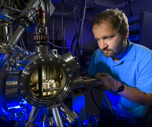
Sandia's Konrad Thürmer (shown here) and Norm Bartelt pushed the boundaries of scanning tunneling microscopy (STM) to image ice - a material believed to be unsuitable for STM because of its insulating nature. (Photo by Randy Wong)
Download 300dpi 6MB JPEG image (Media are welcome to download/publish this image with related news stories.)
LIVERMORE, C.A. — Taking images of ice a few nanometers thick as it forms bulk ice was supposed to be impossible. A scanning tunneling microscope (STM) shouldn’t work with ice because STMs create images by relying on conducting current, which runs contrary to one of ice’s basic properties—insulation.
But that – successfully using an STM to image ice – is precisely what Sandia National Laboratories physicists Norm Bartelt and Konrad Thürmer did.
“How water interacts with solids is extremely important,” says Bartelt. He points to the design of fuel cells and water purification systems as two areas that could benefit from new STM information. “Getting direct information is difficult, so imaging how small ice crystals grow on solid surfaces is an important advance. This is solid information that allows basic theories to be verified. This was our goal—to provide unambiguous information.”
Ice Cubes or Snowflakes?
Bartelt’s and Thürmer’s research was motivated by Sandia colleague Peter Feibelman’s theoretical research in water–solid interactions. In 2002, Feibelman had a major breakthrough in interpreting water–solid interactions. His research explained why an initial layer of water molecules lies flat on the precious metal ruthenium.
The ice-growth images answer a fundamental mystery about ice: snowflakes form in the classic six-sided symmetrical shape, but at low temperatures, ice grows in a cubic form. This phenomenon is something that has puzzled scientists for 60 years.

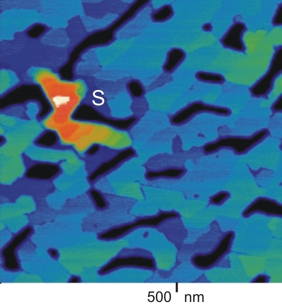
Konrad Thürmer's images reveal that ice grows faster around screw dislocations leading growth spirals (labeled "S"), where cubic ice is being produced.
(Media are welcome to download/publish this image with related news stories.)
What Bartelt and Thürmer discovered was that when an ice film is extremely thin, measuring an average of about one nanometer thick, the water molecules form small, tabular islands of crystalline ice. Once the thickness reaches four or five nanometers, the ice islands join together and start to form a continuous film. In a recent Physical Review B paper, the researchers showed that cubic ice forms when the ice crystals merge. Because of a mismatch in the atomic step heights of the platinum substrate relative to ice, the coalescence often creates screw dislocations in the ice. Further growth occurs by water molecules attaching to the steps that spiral around screw dislocations, creating cubic ice in the process.
Pushing the Boundaries of STM
The STM is a notoriously finicky piece of scientific equipment, and working with ice only increased the difficulty. An STM functions by positioning a sharp, needle-like tip near the sample and then allowing a tiny electrical current to flow across the gap. As the tip of the STM is scanned across the sample surface, the voltage required to position the scanner is used to form an image of the sample.
“Typically, an STM only works if the substrate is conductive,” says Bartelt. Through persistence and patience, Thürmer learned that to image ice, one needs a current smaller than had previously been tried — in fact, three orders of magnitude smaller than what is normally used.
It was Thürmer’s intuitive decision to change the STM’s parameters, namely those for voltage and current, that made imaging ice crystals feasible. Basically, Thürmer found the sweet spot where none was believed to have existed.
The STM was developed in 1981 and earned its inventors, Gerd Binnig and Heinrich Rohr, a Nobel Prize for physics in 1986. “The discovery caused a rebirth of surface science and completely changed the field, but until now, people had not been able to apply it to ice,” says Bartelt. “The fact that we can apply these same methods to ice is very exciting.”
STM experiments don’t always work. “Because you are trying to get atomic resolution, a few atoms on the apex of the tip can completely throw off the experiment,” says Bartelt. “If you are not getting an image, you don’t know if your tip is bad or you are choosing the wrong parameters.”
In fact, the two physicists never expected that they could image thick ice films; they were hoping for a few molecules. Thürmer explains that even after he began imaging thicker ice films, he didn’t trust the results. Instead, he thought they were just misleading electronic artifacts.
Because Thürmer only expected to see films a few molecules thick, he had the STM tip set too close; it was shaving off the top of the films. “For about a month, we thought the films were not really as high as they seemed. We thought the insulating quality of ice made them appear to be higher,” he explains. “I increased the voltage, and the ice appeared to really pop out. Still, I thought it was just the same electronic artifact.”
However, the researchers could not come up with another explanation for why the films appeared so high. Thürmer then purposely grew very thick films and reversed the polarity on the STM, which resulted in an ice carving that proved the thickness was, in fact, real.
The two Sandians are not resting on their initial success; in fact, the two physicists say they are working to build on their breakthrough. Future experiments include putting salts on an ice crystal to see how salts change the crystal’s growth and depositing molecules that react with water, such as atomic oxygen, to determine the exact point on the surface where water dissociates.
“Our ability to image these ice films opens the door to a multitude of exciting new experiments,” says Thürmer.
Sandia is a multiprogram laboratory operated by Sandia Corporation, a Lockheed Martin company, for the U.S. Department of Energy’s National Nuclear Security Administration. With main facilities in Albuquerque, N.M., and Livermore, Calif., Sandia has major R&D responsibilities in national security, energy and environmental technologies, and economic competitiveness.
Sandia news media contact: Mike Janes mejanes@sandia.gov,
(925) 294-2447