NEWS RELEASES
FOR IMMEDIATE RELEASE
July 1, 2008
Sandia wins three R&D 100 awards
Subject areas diverge widely

Water harvested on a surface patterned to mimic the back of the Namib Sternocara Desert beetle. Download 300dpi 2.5MB JPEG (Media are welcome to download/publish this image with related news stories.)
ALBUQUERQUE, N.M. —Every 12 months, teams of experts selected by Chicago-based R&D Magazine name their choices of the year’s 100 most outstanding advances in applied technologies.
Sandia National Laboratories researchers — competing in an international pool that includes universities, private corporations, and government labs — this year were selected for three of those 100 awards.
They were for the Xyce™ Parallel Electronic Simulator 4.0.2, submitted by Eric Keiter; the Silicon Micromachined Dimensional Calibration Artifact for Mesoscale Measurement Machines, submitted by Hy Tran; and the Superhydrophobic Coating, submitted by Jeff Brinker.
“This is yet the latest example of how the Department of Energy and our national laboratories are continuing to demonstrate world-class leadership in innovation, as we enhance our energy security, national security, and economic competiveness,” Energy Secretary Samuel Bodman said. “On behalf of the Department, I would like to congratulate all of our employees who have earned R&D 100 awards and in particular this year’s winners.”
Sandia is a National Nuclear Security Administration laboratory.
The program became available from Sandia in 2007 on a case-by-case basis for commercial and research licenses.
(Media are welcome to download/publish this image with related news stories.)
A coating that really, really doesn’t like water
A transparent coating that isn’t just impermeable to water but actually makes it bounce off a surface has a number of potentially interesting applications. It could prevent corrosion, protect electronics and antiquities, or provide a new, more efficient surface to collect pure water. Modeled from Nature — the lotus leaf’s micro-craggy roughness and the hydrophobic regions of the Namib Sternocara Desert beetle — the Brinker group used sol-gel chemistry to make a patent-applied-for, simple-to-prepare coating solution that, upon simple drying, develops a nanoscopically rough silicon dioxide surface decorated with hydrophobic (water-hating) ligands. The coating can be applied by any standard method — including spin-coating, dip-coating, aerosol spraying, and ink-jet printing — to any surface regardless of composition, size, and shape. An additional benefit is its nearly perfect optical clarity, important for applications like self-cleaning, non-fogging displays, avoiding ice formation on optical elements, and protecting — in a transparent fashion — culturally important statuary from acid-rain corrosion. Importantly the contact angle of the water droplet can be patterned with light to vary from a sphere to a pancake and to control whether and where a drop may roll. Competing hydrophobic products on the whole require very complex processing, are often opaque, and are generally substrate specific. Furthermore they do not provide optically defined spatial control of the coating’s love-hate relationship with water.
Groups led by Brinker have won three R&D 100 awards.
Simulating extremely complex circuits
Xyce is the world’s first analog tool capable of full simulation of large digital circuit systems through the use of massively parallel computation, rather than resorting to accuracy-compromising simplifications used by other tools. Given the complexity of large-scale integrated circuits, trial-and-error circuit testing is prohibitive and lower fidelity digital simulation fails to take effects like parasitic currents and electrical—interconnects into sufficient account. Existing analog simulators are limited to single processor workstations. Xyce, under development at Sandia since 1999, accurately simulates more than 10 million circuit elements on hundreds of processors, far exceeding any other simulation tool. Originally used to help certify integrated circuits in the presence of radiation and other hostile effects, today it also helps the electronics industry create simulations that cope accurately with decreasing feature size and the increasing number of integrated circuit components.
Calibrating with nanoscale accuracy
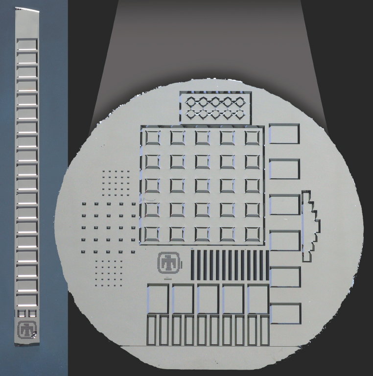
The Sandia Hybrid Dimensional Calibration Artifact for a 3-D workspace is made from single-crystal silicon, patterned and then anisotropically etched to form a variety of features. The edges of these features are sharp at the nanometer scale and fabricated on a 150-mm-diameter single crystal silicon wafer.
Download
300dpi 2.5MB JPEG
(Media are welcome to download/publish this image with
related
news stories.)
To calibrate a device, an accurate calibration artifact is of primary importance. The Silicon Micromachined Dimensional Calibration Artifact for Mesoscale Measurement Machines has a long title but will help improve measurement accuracy for producing miniaturized devices such as fuel injectors, watch components, and inkjet printer parts as these high-volume parts are being manufactured. The Sandia MEMS-based three-dimensional physical artifact is 10 times more accurate and much less expensive than the former gold (so to speak) standard of patterned chrome on glass – a fundamentally two-dimensional device lacking the ability to be calibrated by high-accuracy methods. The Sandia artifacts, formed through the classic MEMS technology of anisotropic bulk micromachining, have nanometrically sharp, long-lasting crystalline edges that are macroscopically long. Such artifacts can be used to calibrate a variety of inspection systems.
The R&D 100 awards — occasionally referred to as “the Nobel Prizes of technology” — were first awarded in 1963 as the I-R 100s, in keeping with the original name of the magazine, Industrial Research.
Many entries over the ensuing years became household names, including Polacolor film (1963), the flashcube (1965), the automated teller machine (1973), the halogen lamp (1974), the fax machine (1975), the liquid crystal display (1980), the printer (1986), the Kodak Photo CD (1991), the Nicoderm antismoking patch (1992), Taxol anticancer drug (1993), lab on a chip (1996), and HDTV (1998).
The sole criterion for winning, according to a description released by the magazine, is “demonstrable technological significance compared with competing products and technologies.” Properties noted by judges include smaller size, faster speed, greater efficiency, and higher environmental consciousness.
Winners are presented plaques at a formal banquet in Chicago in early fall.
Sandia is a multiprogram laboratory operated by Sandia Corporation, a Lockheed Martin company, for the U.S. Department of Energy’s National Nuclear Security Administration. With main facilities in Albuquerque, N.M., and Livermore, Calif., Sandia has major R&D responsibilities in national security, energy and environmental technologies, and economic competitiveness.
Sandia news media contact: Neal Singer, 505-845-7078, nsinger@sandia.gov