Download 300dpi JPEG image, ‘fivelayer.jpg’, 1Mb (Media are welcome to download/publish this image with related news stories.)
ALBUQUERQUE, NM — A new advanced five-level polysilicon surface micromachining process pioneered at the Department of Energy’s Sandia National Laboratories promises that microelectromechanical systems (MEMS) of the future will be more reliable and capable of doing increasingly complex tasks.
“This five-level polysilicon surface micromachining technology has potential of becoming the industry standard, replacing the more commonly used two- or three-level polysilicon surface micromachining approaches,” says Steve Rodgers, Sandia engineer who together with colleague Jeff Sniegowski has spent the past several years prototyping designs and developing the innovative process. “We have been working hard to baseline the technology as a reproducible manufacturing process, and we’re getting there.”
The new technology was developed at Sandia’s Microelectronics Development Laboratory. MEMS devices made from the five-level process will eventually be manufactured in the new Microsystems and Engineering Sciences Application (MESA) facility being planned for construction at Sandia.
MEMS, complex machines with micron-size features, can be found in a variety of products, including optical devices, computer game joy sticks, car airbag sensors, inkjet printers, projection displays and more. They are so small that they are almost imperceptible to the human eye and have moving parts no bigger than a red blood cell.
Sandia will begin offering the five-level technology next spring to external customers for prototyping purposes. Information about all MEMS courses is available at Sandia’s micromachine Web page located at http://www.mdl.sandia.gov/micromachine.
Almost all of today’s surface micromachine components are designed for and fabricated in technologies that incorporate three or fewer levels of structural materials. The levels are typically deposited as thin films of polysilicon that are about one to two microns thick. These films are separated by air gaps that are initially defined by layers of sacrificial silicon dioxide (sacrificial because they will eventually be eliminated) of about the same thickness. Processes with thicker polysilicon film — up to tens of microns — exist, but are typically limited to only that layer.
“In general, the more layers of structural material that a designer has to work with, the more complicated the device that can be fabricated,” says Sniegowski, who developed the fabrication technology for the five-level layering method. “Therefore, surface micromachined components have greater functionality than bulk micromachined parts.”
He adds that’s why the five-level polysilicon surface micromachine process that incorporates four layers of structural films plus an electrical interconnect layer is so attractive.
“This technology permits mechanical functionality that only a five or more layer process could offer,” Sniegowski says.” It provides a base for designing truly sophisticated multilevel microelectromechanical systems, while simultaneously offering much of the yield and robustness that is typically associated with single-level micromachining technology.”

Download 300dpi JPEG image, ‘5_level.jpg’, 612K (Media are welcome to download/publish this image with related news stories.)
A two-level polysilicon process has only one layer of structural material, with the other level defining the ground plane. Such a technology is useful for fabricating simple sensors and actuators.
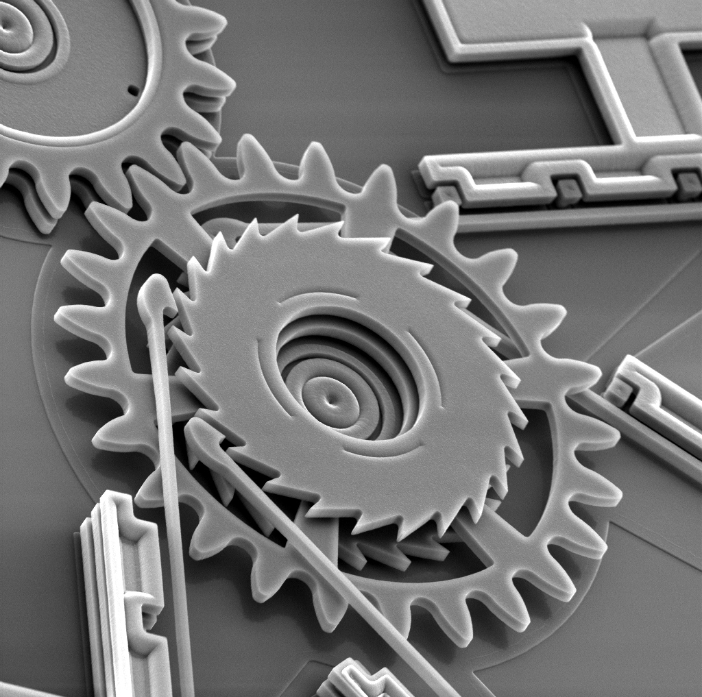
With three levels it is possible to create gears with hubs, while the four-level technology provides an additional layer of material that can be used to define linkage arms that move above the plane of the gears, enabling a continuous 360-degree rotation.
The five-level technology expands on this to permit complex interacting mechanisms to be fabricated on moving platforms.
But to do this, several challenges had to be overcome, which Sniegowski and Rodgers have met. For example, as additional layers are added, more texture appears on the surface. This occurs because the top layer acquires the characteristics of all the lower layers, including high and low spots. The result is the creation of protrusions, called “mechanical parasitics,” that extend from the upper mechanical layer to lower areas. They can interfere with operation.
These parasitics, Sniegowski says, can significantly “constrain the design.” If the design doesn’t take them into account, they could easily “collide with the teeth and prevent rotation of the gear.”
To eliminate this problem, a Sandia team led by process engineer Dale Hetherington modified and patented a process commonly used in manufacturing integrated circuits — chemical mechanical polishing — to planarize (flatten) the surface. High spots are eliminated after a very thick layer of sacrificial oxide covers all previous layers. Through chemical mechanical polishing, the high spots are eroded, producing a uniform flat surface.
Rodgers says the new five-layer process provides a foundation for fabricating components that offer high performance, reliability, and robustness. However, work continues to improve the process even further.
“We are now adding the final touches before offering it for widespread use,” he says.
