ALBUQUERQUE, N.M. — Tungsten-filament bulbs — the most widely used light source in the world — burn hands if unscrewed while lit. The bulbs are infamous for generating more heat than light.
Now a microscopic tungsten lattice — in effect, a tungsten filament fabricated with an internal crystalline pattern — developed at the Department of Energy’s Sandia National Laboratories has been shown to have potential to transmute the majority of this wasted infrared energy (commonly called heat) into the frequencies of visible light.
This could raise the efficiency of an incandescent electric bulb from 5 percent to greater than 60 percent.
By doing so, it would greatly reduce the world’s most vexing and important power problem — the required excess electrical generating capacity and costs to homeowners caused by inefficient lighting, as well as the environmental damage accompanying unnecessary power generation.
The advance also opens the possibility of increased efficiencies in thermal photovoltaic applications (TPV). Photovoltaics work best when they are provided with energy from heat-generators with energy emission wavelengths transposed into the most optimal frequencies. (Using a tungsten lattice as an emitter at desirable frequencies, model calculations showed that the TPV conversion efficiency reached 51 percent compared with 12.6 percent efficiency with a blackbody emitter.)
The first step toward this goal, achieved at Sandia by Shawn Lin and Jim Fleming, is reported in the May 2 Nature.
Fabrication of the device was accomplished by an extension of well-known MEMS (microelectromechanical systems) technologies that themselves have been derived from mature semiconductor technologies. As a result, fabrication of such devices could be cheap and easy.
History of photonic lattices
Since the existence of photonic crystals was postulated by Eli Yablonovitch of UCLA more than a decade ago, the most common idea for their use was based on their capability to transmit beams of light at selected frequencies and bend their paths without losing any energy. The structures, most often made out of silicon, consist of tiny bars fabricated to sit astride each other somewhat like Lincoln Logs at regular pre-set distances and angles that form in effect an artificial crystal. Spacing of the bars allows passage of only certain wavelengths; other wavelengths too big for the rafters, so to speak, cannot pass through. Desirable wavelengths not only pass through but also can be changed in direction by creating defects in the artificial crystal that cause the light to follow the defect along like a car passing through a curving tunnel. This meant photonic crystals had potential in optical communications, in which light beams currently carrying telephone messages and data must be converted to electrons — an expensive process — for certain tasks.
Meltdown? Apparently not
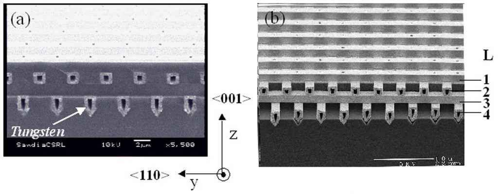
A further question considered by Lin and Fleming, with assistance from colleagues Ihab El-Kady, Rana Biswas, and Kai-Ming Ho at Ames Laboratories in Iowa, shifted emphasis from a photonic lattice’s ability to guide light to its capability of stopping other frequencies from passing through it. What happens to these other energies that enter the interior of a three-dimensional crystal? If the crystal were built of tungsten — fabricated by creating a structure of polysilicon, removing some silicon and using chemical vapor deposition to deposit tungsten as a kind of backfill in the mold — the metal could handle quite high temperatures and have a large and absolute photonic band gap in the visible range where it is already known to emit light. But what would happen to the other, lower-wavelength energies brought in by an electric current? Would the structure melt through the buildup of heat? Or, more desirably, would the thermally excited tungsten atoms somehow prefer to reinforce emissions at higher wavelengths, such as in the visible frequency range?
Energy at the edge of the photonic band was observed to undergo an order-of-magnitude absorption increase, or enhancement. This meant that energy was being preferentially absorbed into a selected frequency band. Meanwhile periodic metallic-air boundaries led to an extraordinarily large transmission enhancement. Experimental results showed that a large photonic band gap for wavelengths from 8 to 20 microns proved ideally suited for suppressing broadband blackbody radiation in the infrared and has the potential to redirect thermal excitation energy into the visible spectrum.
The imaginative work seems logical in retrospect, though the theory for the effect — re-partitioning energy between heat and visible light — remains unexplained. “It’s not theoretically predicted,” says Fleming. “Possible explanations may involve variations in the speed of light as it propagates through such structures.”
The work was performed with a photonic crystal operating in the mid-infrared range, but no theoretical or practical difficulties are known to exist to downsizing the structure into the visible light range.
All work was performed on commercially available, monitor-grade 6-inch silicon wafers. These photonic devices were fabricated in Sandia’s Microelectronics Development Laboratory using modifications of the standard CMOS processes originally developed for Sandia’s radiation-hardened CMOS (complementary metal-oxide semiconductor) technologies.
The work was funded by the Laboratory-Directed Research and Development program through project manager James Gee. Co-principal investigator Jim Moreno modeled.
For information on Sandia’s solid-state lighting project visit the web site at http://lighting.sandia.gov.
