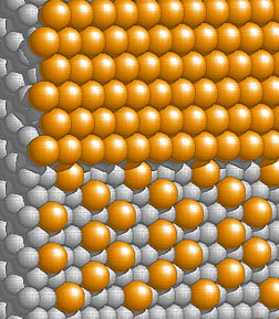
Download 300dpi JPEG image, ‘Kellogg_Fig2.jpg’, 172K (Media are welcome to download/publish this image with related news stories.)
ALBUQUERQUE, N.M. — Coffee beans spilled upon a table form no pattern, they’re a mess, their distribution dictated by the laws of chance. The same was generally believed true of atoms deposited upon a substrate. Now, the first vision of a peaceable kingdom in which deposited atoms form orderly, controllable 2-D nanopatterns has been observed by researchers at the Department of Energy’s Sandia National Laboratories.
Pattern control at this level means that nanotemplates could be formed to fine-tune the device characteristics of self-assembling nanostructures. Possibly, characteristics could be tailored for devices like photonic lattices, an advanced method for controlling light and of wide interest to the huge telecommunications industry.
The work, described in the Aug. 30 Nature, produced real-time video of atoms self-arranging themselves in the manner long predicted by a variety of theorists but contrary to ordinary intuition. Thus, such theories generally had been treated with a great deal of skepticism, says Sandia physicist Norm Bartelt: “There was no obvious route for atoms to arrange themselves in predicted patterns.”
Says Sandia researcher Richard Plass, “Kinetics say that 10,000 moving atoms should go anywhere. Nobody really expected an assembly would arise.”
Observation of the real-time assembly process, along with control over physical factors that influence that process, offer a means of finding out far more about the conditions under which atoms self-assemble than any theory could predict, and thus, how to influence that assembly into more desirable structures.
“There are many control knobs we can turn to create new patterns,” says Bartelt. Among them are temperature and material composition.
The researchers observed atoms of lead deposited on a copper substrate forming, first, lead dots, then lead stripes, and then reverse dots — copper becoming the dot material — as more lead is added.

Download 300dpi JPEG image, ‘Kellogg_Fig1.jpg’, 508K (Media are welcome to download/publish this image with related news stories.)
“The work — which to our knowledge is the first unambiguous observation of the expected sequence of domain patterns — helps understand the new physics that manifests itself at these small length scales,” says Sandia project lead Gary Kellogg. “New materials with highly specialized properties necessary to meet defense and consumer needs can be fabricated only by tailoring the structure of the material on the nanometer scale. This work provides insight into how nature does this, and how humans can do the same.”
Sandia researchers were able to record real-time, real-space images using a low-energy electron microscope (LEEM) that show exactly how the nanostructures are generated, self-assemble, and transform. “The close agreement between experiment and theory allows us to probe the key inter-atomic force parameters involved in the process,” says Kellogg.
Theorists long have believed that competing attractive and repulsive inter-atomic interactions can lead to the spontaneous formation of ordered patterns in widely varying chemical and physical systems. Potentially, such patterns could be used as templates for nanostructure fabrications.
“There are precedents for people using these patterns for further growth of quantum dots,” says Bartelt. “They can be the starting point of controllable patterns that extend into three dimensions.”
Though models have clearly predicted the possibility of controlling any pattern’s geometry and order, depending on temperature and amount of secondary metal introduced, experimental verification of these models had remained elusive till now.

