Download 150dpi JPEG image, ‘microsub.jpg’, 608K
ALBUQUERQUE, N.M. — In a few years a dime-size microchip may be home to as many as 10 million transistors. But the electrical resistance created as all those snug circuits zap electrons back and forth are causing even today’s tightly packaged microprocessors to get hot — really hot.
That’s a problem for owners and makers of computers, cell phones, and other computerized electronic devices. Hot microchips and printed circuit boards fail faster as their tiny interconnects succumb to the rigors of cyclic heating and cooling. More damaging are temperature differences, or gradients, across chips that can cause tiny cracks and stress voids to form in a chip’s delicate wiring.
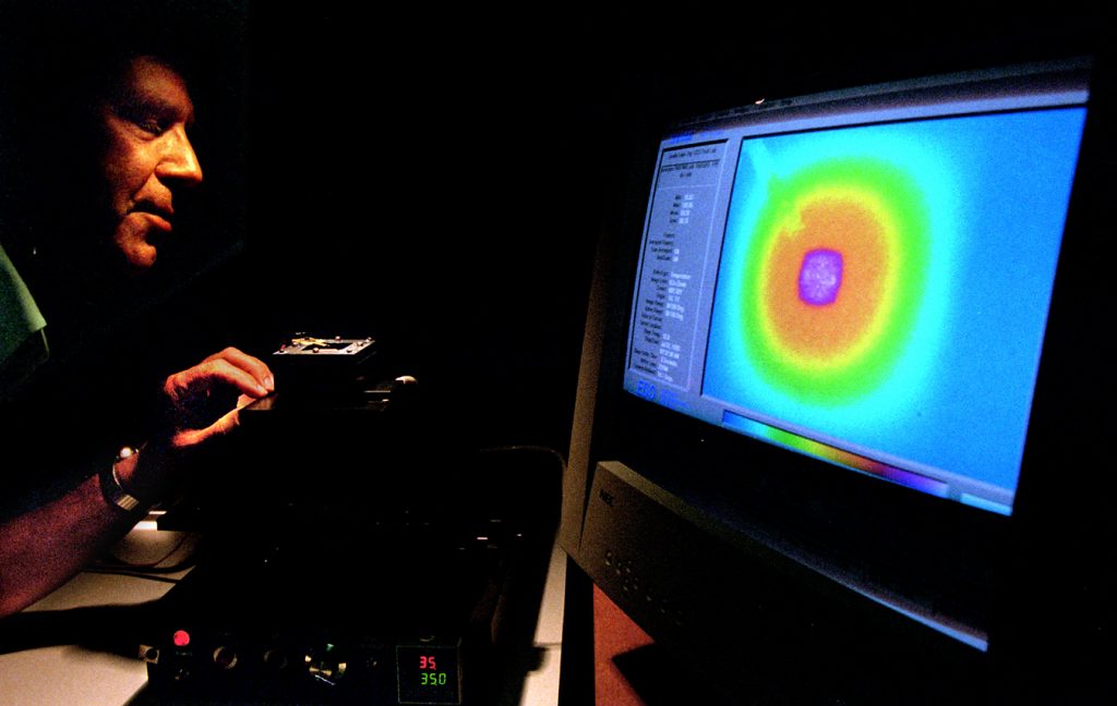
Researchers at Sandia National Laboratories, a U.S. Department of Energy research and development lab based in Albuquerque, N.M., have developed an innovative substrate that removes heat from microchips and printed circuit boards and keeps them closer to their optimum operating temperatures. The Sandia approach makes use of an intricate network of microscopic, coolant-filled passages formed directly within the substrate.
Finding affordable heat removal a major challenge
Although various heat-removal methods have been devised for high-end microelectronics devices such as military satellites and radars, they aren’t applied to everyday electronics because they’re too expensive. As the chips in lower-end devices get smaller and operate hotter, even the most common devices, including desktop computers and cell phones, may soon require heat dissipation technology, says David Benson of Sandia’s Advanced Packaging Department.
“Heat buildup is becoming one of the major limitations to creating tomorrow’s more compact, complex micro devices,” he says.
Traditionally microchip substrates are made of fiberglass-epoxy-type materials laden with copper interconnects that help conduct heat into the substrate and away from the microchip. Other designs include supplementary heat spreaders of solid copper or other conductive materials within the substrate. In the recent past, highly conductive diamond and diamond-coated substrates have been developed, but their use is drastically limited by their high cost.
And as chips get hotter, simple conduction in affordable materials won’t do the job, David says.
To solve the heat-buildup problem in specialty microelectronic devices and some laptop computers, microchip manufacturers have added small tubular heat pipes to the surfaces of microchips that help carry some heat away from the hottest circuitry and transfer it to other structural elements, such as a printed circuit board’s external surfaces. But the surface connections where tubular heat pipes meet substrate typically conduct heat very poorly and therefore aren’t effective heat removers.
In the new Sandia substrate, the “micro heat pipes” built directly within the substrate material carry heat away from the chip much more efficiently than conduction through solid copper or transport through larger heat pipes on the substrate surface and thus allow for greater heat reduction and improved temperature control.
“Sandia put the cooling right where the action is,” Benson says. “The closer the coolant is to the circuit, the more heat can be managed.”

The world’s smallest waffle iron
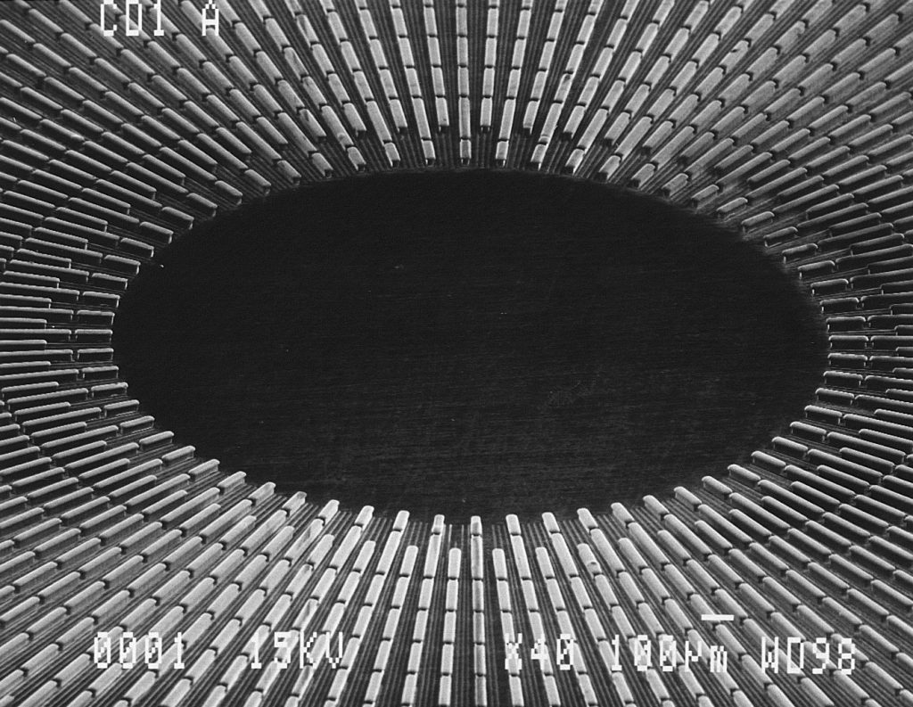
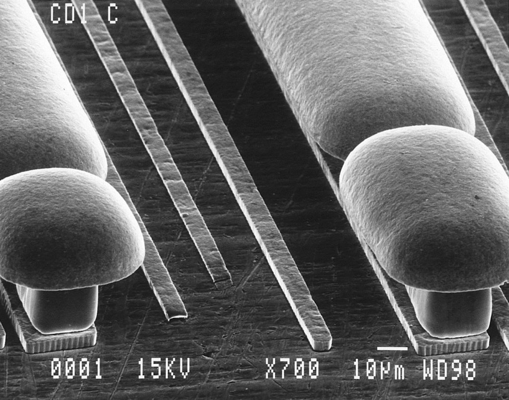
To make the subsurface micro pipes, researchers in Sandia’s Compound Semiconductor Research Laboratory developed a process for adding, through a repetitive photolithography-electroplating process, 5- to 50-micron-wide ridges on the surfaces of two metal alloy plates. The built-up patterns on each plate are mirror images of one another. When the plates are put together, tiny passages remain between them, much like the spaces between the top and bottom halves of a waffle iron where the waffle is baked.

Download 150dpi JPEG image, ‘heatpip2.jpg’, 810K
Download 150dpi JPEG image, ‘heatpip1.jpg’, 743K
The plates’ edges are then sealed together, resulting in a metal sheet five-one-hundredths of an inch thick containing an interconnected network of micron-scale galleries.
A quarter-million structures have been created within a square inch of the substrate.
Inside the substrate the researchers inject a small amount of liquid coolant — a few drops at most. As the coolant directly underneath the operating microchip heats up and evaporates, it moves through the galleries to cooler areas, where it recondenses, distributing its heat throughout the substrate. Capillary pressures on the recondensed liquid then pull the coolant back to hotter regions where evaporation has occurred, similar to the way a candle wick draws molten wax upward to the flame.
“The amount of capillary pressure inside the tubes is a function of the size of the passages,” Benson says. “As the structures get smaller, more pumping action is created within the substrate.”
This cyclic evaporation and condensation effect distributes heat throughout the substrate much more efficiently than simple conduction through a solid, Benson says.
“It’s a weather microcosm under a chip,” he says.
A coolant and micropipe geometry can be selected that best transfers heat given each device’s design and operating temperature range.
A Sandia patent on the technique is pending.
Inexpensive, durable, malleable, bondable
In laboratory tests, samples of the Sandia substrate reduced the operating temperature of chips by twice as much as commonly used substrate materials. It also spread the heat throughout the substrate more uniformly, eliminating hot spots that can damage a chip.
The iron-nickel alloy used in the initial design bonds well to silicon chips, although the micro pipe substrate could be made from a variety of materials, Benson says. The micro heat pipe substrates also are “passive” devices, meaning no pumps or other mechanical actuators are required to make them work.
The substrates are surprisingly durable, they can be stamped into a variety of shapes and sizes (to match compact devices such as cell phones, for instance), and, most important, they are simple and cheap to manufacture in bulk. Sandia estimates a production cost of about 50 cents per square inch of the higher-performance micro heat pipe substrate, compared to more than $1 per square inch of current affordable, high performance electronic packaging materials.
The substrates’ cooling efficiency can increase the reliability and life span of components in computers, communications satellites, photovoltaics, and radar applications as well, he says.
“This is an example of a national laboratory technology that may have both commercial and specialized defense-related applications,” Benson says.
Sandia is working to license the technology to a small microelectronics packaging firm in California. Cooperative research and development agreements (CRADAs) also are being discussed with end users in the U.S. microelectronics industry.
Researchers and companies interested in this technology should contact:
Angelo Salamone, alsalam@sandia.gov, Partnering and Licensing Department, Sandia National Laboratories (505) 843-4146
