Download 150dpi JPEG image, ‘lattice.jpg’, 736K
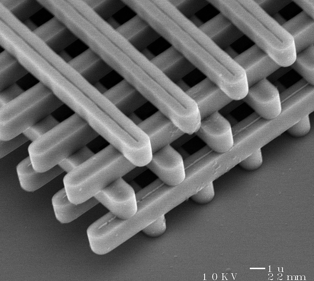
ALBUQUERQUE, N.M. — By interlocking tiny slivers of silicon into a lattice that, under a microscope, appears to be formed by toy Lincoln Logs, scientists at the Department of Energy’s Sandia National Laboratories believe they have solved a major technical problem: how to bend light easily and cheaply without leaking it, no matter how many twists or turns are needed for optical communications or (potentially) optical computers.
The lattice, dubbed a photonic crystal (crystals have regularly repeating internal structures), now works in the infrared range (approximately 10-micron wavelengths). This achievement is of military and commercial interest because the technique can be used to enhance or better transmit infrared images.
Sandia researchers Shawn Lin and Jim Fleming now are preparing a 1.5 micron crystal — the region in which almost all the world’s optically transmitted information is passed.
The improvement — which bends far more light in far less space at considerably less cost than current commercial methods — will make possible tinier, cheaper, more effective waveguides to combine or separate optical frequencies at the beginning or end of information transmissions and find wide application in data transmission and in more compact and efficient sensors. (See “Technique perfected….” backgrounder that follows.)
Pierre Villeneuve, a research scientist at the Massachusetts Institute of Technology (MIT), says, “With the structure [Sandia researcher] Shawn [Lin] is using now, he’ll be able to hit the 1.5 micron mark within the next 12 months. This shows how ‘key’ this work is: He’s using a technique that lends itself to hitting the mark.”
A venture capitalist requesting anonymity has approached the researchers to commercialize the process.
The achievement, for which Sandia has applied for a patent, was reported in the July 16 issue of the journal Nature.
The structure, in the regularity and spacing of its parts, is mirrorlike in not permitting light of a particular frequency, caught within the cavity of the structure, to escape. Instead, light must follow along any twists or turns designed into the log structure.
By designing the distance between logs carefully, a chosen wavelength is reflected instead of passing out of the space, as longer or shorter wavelengths can. With introduction of an impurity like air or much thicker polysilicon “logs” to provide routes for preselected wavelengths introduced into the crystal, light travels along the impurity as it twists or bends. No matter how sharp the turns, light of frequency roughly in the middle of the band gap cannot escape. Funding for the project was provided by Sandia’s Laboratory-Directed Research and Development office, which funds speculative, defense-related research, and by the DOE.

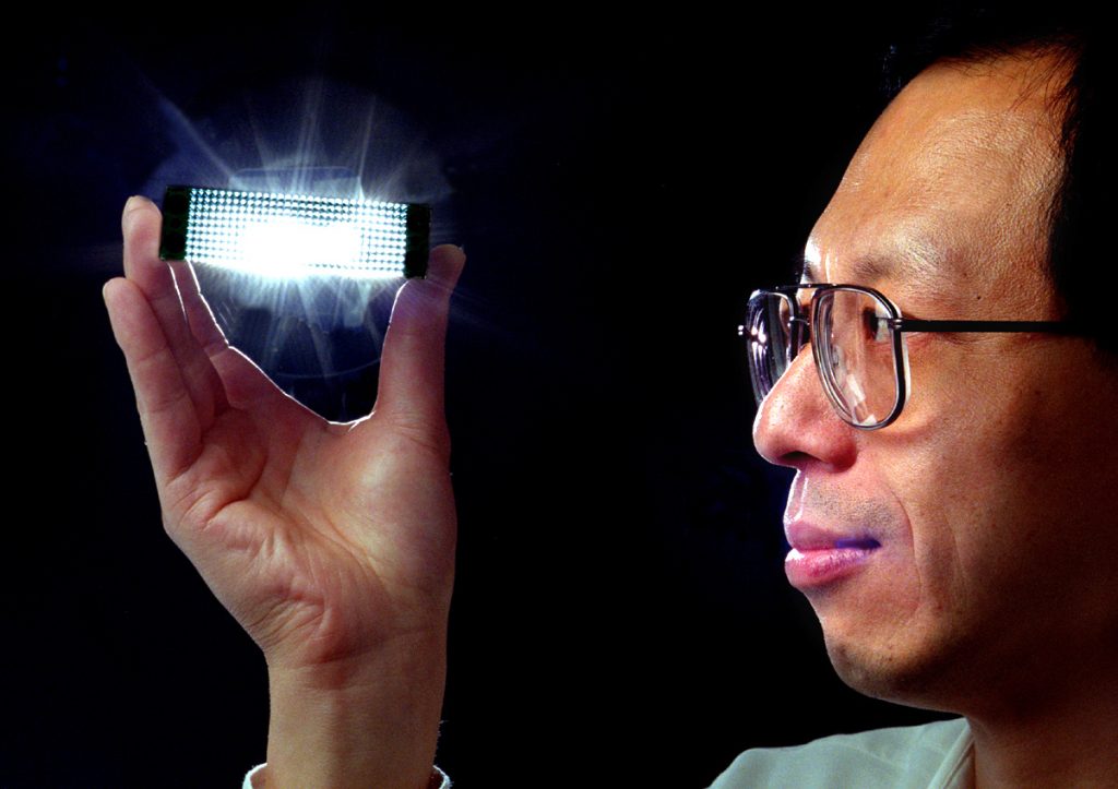
Download 150dpi JPEG image, ‘Shawn.jpg’, 752K
A photonic band gap
What’s cool, in the eyes of some observers, is that Sandia researchers Lin and Fleming have created the equivalent of a photonic “band gap” that forbids certain frequencies of light from exiting the lattice. (“Band gap” is a term usually applied to electrons, not photons, and signifies a range of energies in which electrons are absent because their presence would contradict quantum mechanical laws.)
The nearly leak-proof lattices form a cage that trap and guide approximately 95 percent of the light sent within them, as compared with approximately 30 percent for conventional waveguides, and they take only one-tenth to one-fifth the space to bend the light. (The Sandia photonic lattice’s turning radius is currently in the one-wavelength range, rather than the traditional waveguide bend of more than 10 wavelengths.)
Standard, integrated-circuit manufacturing technology used to fabricate micromachines — machines nearly too small to see — at Sandia’s Microelectronics Development Laboratory can create tens of thousands of waveguides from a single, 6-inch silicon wafer. This is a factor 10 to 100 times more dense than can be fabricated using more expensive gallium arsenide with current commercial technology.
Potential uses: low-energy lasers, photonic computers, communications
Because little light is lost in the three-dimensional mirroring that sends light back at itself, a new type of microlaser requiring little start-up energy is theoretically achievable. (Most conventional lasers require large jolts of energy to begin operating because so much light is lost in the lasing start-up process.)
The achievement also brings nearer the day when computers that transmit information using photons rather than electrons become a practical reality. Currently, desktop computers use electrons to pass information, but as more circuits are included on new chips, they become more difficult to cool. Photons, the stuff of light, are faster and cooler than electrons. The problem is that no one has been able to bend useful frequencies of light around tight corners (as navigated by electrons through a million turns on a computer chip the size of a postage stamp) without incurring large losses in information; with previously used techniques, light leaks, and badly, the more tightly it is turned.
One principle of optical communications is that differing frequencies of light are bent by different amounts. Waveguides first combine the frequencies of a number of information streams — for example, telephone calls — by bending them into the combined “white” light passing through an optical cable; then other waveguides separate the light into component frequencies by bending it at the end of its journey.
Photonic band gap crystals — a history
The idea of a “photonic band gap structure” was first advanced in 1987 by Eli Yablonovitch, now a professor at the University of California at Los Angeles. In 1990, he built the first photonic crystal, baseball-sized to channel microwaves useful in antennae applications. In the mid 1990s, scientists at Ames Laboratory in Iowa built crystals the size of ping pong balls, also for microwaves. The components were of a size that could be put together by hand, using straight metal pins (of the type that hold new shirts in place).
The size reduction for current structures is a striking achievement that researchers have been attempting to achieve for a decade, says Del Owyoung, Sandia manager for the project. The difference in frequency is comparable to moving from masers to lasers, he said — from microwaves to optical waves.
According to Rama Biswa, a researcher at Ames Lab, “We had built the same structure [as Sandia has] ourselves, but more than 100 times larger, in the microwave frequency range. I think it is quite remarkable that Shawn Lin’s group could do it at these wavelengths in the infrared and at this size.” Villeneuve, who has theorized about uses for photonic crystals for much of the 1990s in a group led by MIT professor J. D. Joannopoulos, praised the Sandia group for “showing that what we’re doing is valid,” he says. “[People would say,] ‘It’s wonderful that you’re coming out with all these great devices [that make use of photonic crystals], but your building block doesn’t even exist!'” That is no longer the case.
Sandia is a multiprogram DOE laboratory, operated by a subsidiary of Lockheed Martin Corp. With main facilities in Albuquerque, N.M., and Livermore, Calif., Sandia has major research and development responsibilities in national security, energy, and environmental technologies.
Technique perfected in building surface-etched micromachines
Shawn Lin and Jim Fleming achieved the desired crystalline spacing using techniques perfected in building surface-etched micromachines, at which Sandia is a world leader. Gears that spin require spaces between parts; specifically, a silicon base is covered with an expendable coating in which a part can be etched, and then the expendable portion is removed by chemical and mechanical means, leaving the gear or axle unencumbered by surrounding material and thus able to spin freely [http://mems.sandia.gov/scripts/].
Using a variant on the same technique, Fleming made an artificial crystal lattice. He took a silicon wafer, coated it with silicon dioxide, cut trenches into the silicon dioxide and then bathed the chip in polysilicon till it filled the trenches. Then he polished the surface until smooth and bathed the chip in another layer of silicon dioxide, into which he cut the same number of trenches as before, but so they lay across the trenches beneath them at right angles, and then filled these trenches with polysilicon.
After repeating this process a number of time, Fleming removed the silicon dioxide, using hydrofluoric acid, and got “micron layers of Lincoln Logs, orthogonal to each other, and joined where they touch.”
Center to center, the polysilicon logs were 1.2 microns wide, 1.5 microns high, with a pitch of 4.8 microns — child’s play to achieve in the world of silicon micromachines. The proportions were identical to that specified by Ames Laboratory and Iowa State researchers as those necessary to make the photonic equivalent of an electronic band gap.
Technical contacts:
Shawn Lin, slin@sandia.gov, (505) 844-8097
Jim Fleming, fleminjg@sandia.gov, (505) 844-9158
Del Owyoung, aowyoun@sandia.gov, (505) 884-5481
