ALBUQUERQUE, N.M. — Sandia National Laboratories researchers won seven R&D 100 awards this year — the most the Labs has won since it garnered eight, its most ever, in 1997.
The annual contest, sponsored by the Chicago-based trade magazine R&D Magazine, uses technical experts to help determine the best applied new technologies. One hundred winners are chosen from an international pool of contestants from universities, private corporations, and government labs.
Sandia, a Department of Energy national laboratory, won many of the awards in partnership with private companies, other labs, or universities. Recent emphasis on technology transfer has boosted the number of joint submissions.
The R&D 100 Awards — sometimes referred to by pundits as “the Nobel Prizes of technology” — were first awarded in 1963 as the I-R 100s, in keeping with the original name of the magazine, Industrial Research. Many entries over the ensuing years became household names, including Polacolor film (1963), the flashcube (1965), the automated teller machine (1973), the halogen lamp (1974), the fax machine (1975), the liquid crystal display (1980), the printer (1986), the Kodak Photo CD (1991), the Nicoderm antismoking patch (1992), Taxol anticancer drug (1993), lab on a chip (1996), and HDTV (1998).
The sole criterion for winning, according to a description released by the magazine, is “demonstrable technological significance compared with competing products and technologies.” Properties noted by judges include smaller size, faster speed, greater efficiency, and “higher environmental consciousness.”
The magazine has responded to new technologies by creating additional categories. Winners have been chosen in the fields of analytical instruments and processes, electronics, testing and measurement, software, environmental technology, and advanced biomedical devices and systems.
Winners will be presented plaques at a formal banquet in October at Chicago’s Navy Pier.
Here are brief descriptions of the seven winning Sandia technologies:
SnifferStar
It’s hard enough to keep track of where you are on a battlefield. Imagine trying to keep track of what you are breathing.
Helping US forces of the future may be an extremely lightweight mobile chemical sensor created by Doug Adkins with George Dulleck, Greg Frye-Mason, Pat Lewis, Richard Kottenstette, Edwin Heller, Ronald Manginell (all Sandians), and Clifford Megerle, formerly a Senior Technical Staff Member at Lockheed Martin.
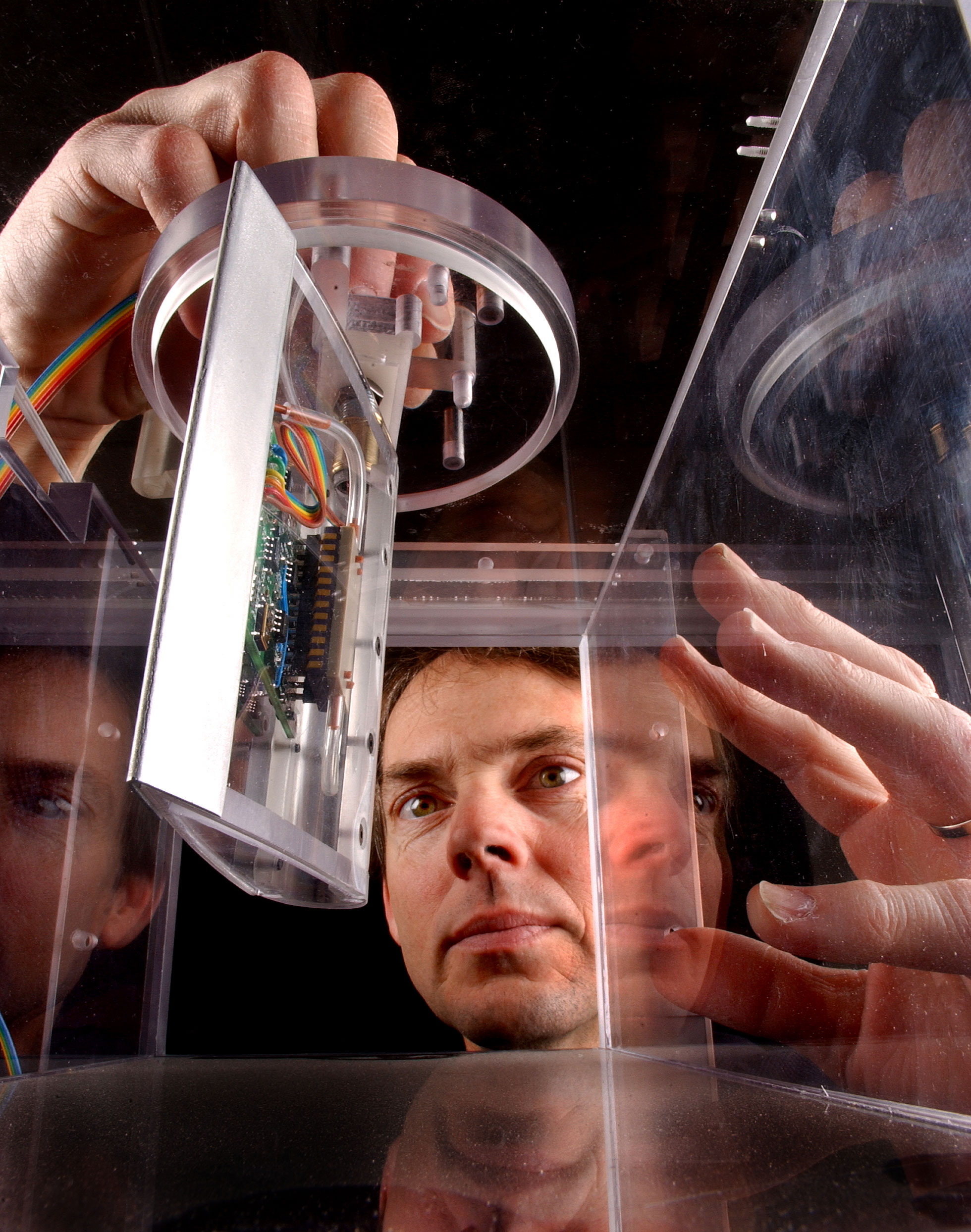
SnifferStar™ mounts on a drone aircraft for remote surveillance of battlefield situations where suspect plumes or clouds are present. The detector’s primary purpose is to save lives by warning soldiers that chemical weapons are present on a battlefield. Developed under a Shared Vision program with Lockheed Martin, the entire module weighs less than a golf ball, operates on less than 0.5 watts, and uses the wind generated by the motion of the craft to collect samples for analysis. SnifferStar™ is sensitive to both blister and nerve agents. It ignores common interferents and analyzes chemical warfare agents in 20 seconds.
Says Adkins, “Such rapid analysis currently is not possible with any other package near this size.”
The device also has possibilities for use in or near the ventilation systems of buildings, or, with addition of small pumps to force air into the device, on posts surrounding military bases.
Extreme Ultraviolet Lithography Full-field Step-Scan System
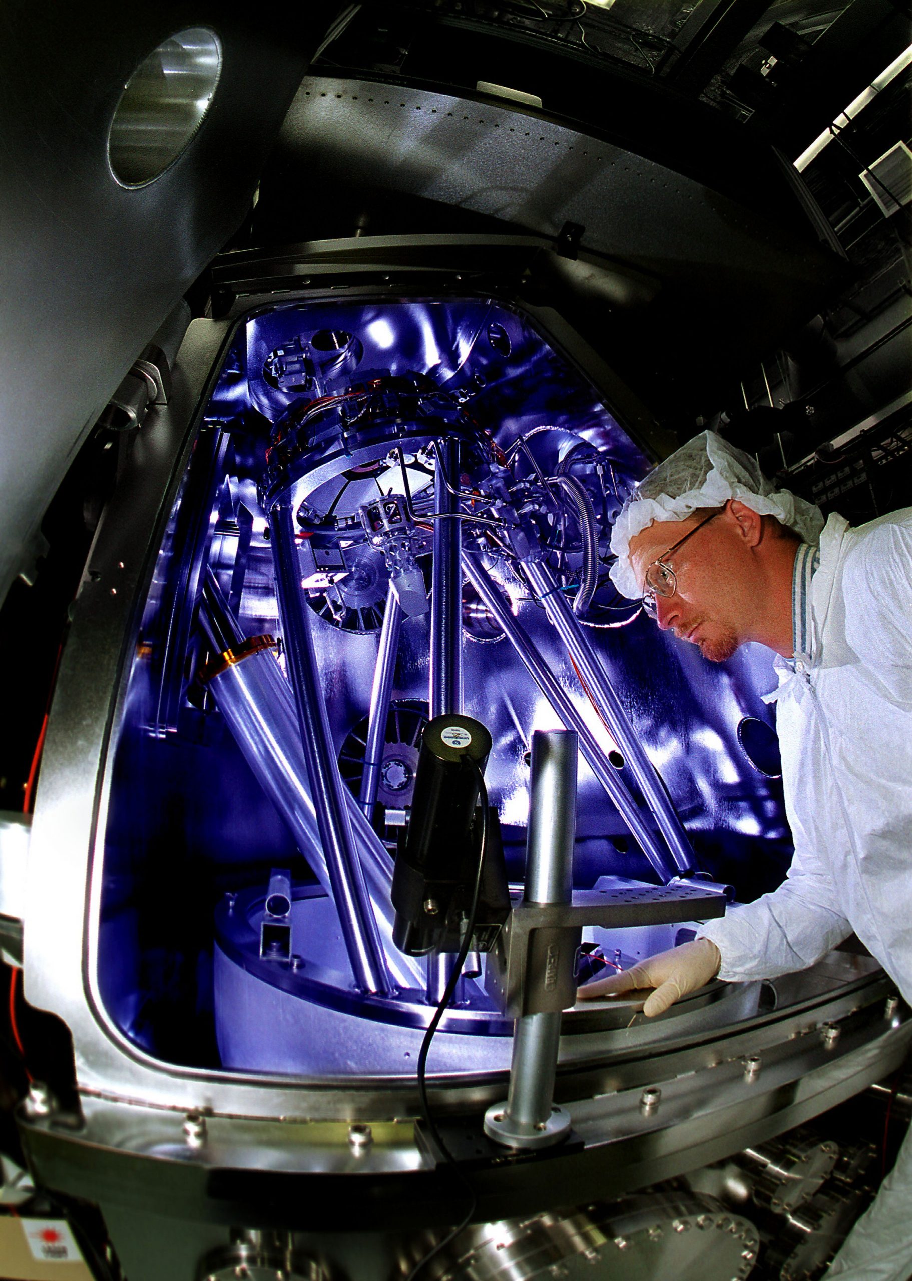
More than 50 Sandians and collaborators from Lawrence Livermore (LLNL) and Lawrence Berkeley national laboratories were honored for this technological advance that will lead to dramatic improvements in the speed and memory of computer systems. Researchers created the only system that can pattern full chip-size areas on silicon wafers with features as small as 50 nanometers. It is the embodiment of a set of groundbreaking technologies that were considered by many to be impossible as recently as a few years ago. Commercialization of this breakthrough will allow advances in microelectronics to continue into the next decade.
In addition to the national laboratory team, the award is being given jointly to Northrup Grumman Space Technology/Cutting Edge Optronics. The work was done in partnership with an industrial consortium comprising Intel, Motorola, AMD, Infineon, IBM, and Micron. Intel ordered the first production-level instrument based on this technology last year.
Acoustic telemetry technology

Acoustic telemetry technology, developed at Sandia in cooperation with Extreme Engineering Ltd. of Calgary, Alberta, and with support from DOE, represents the fulfillment of an oil industry quest that goes back to the 1940s.
The problem: As oil and gas wells have gone deeper and deeper, the need for better communication between the driller and the drill bit has become more critical.
Standing next to a drilling rig, you see a simple well head; beneath your feet, well-casing strings, production tubing, and other drilling equipment extend miles beneath you, often reaching “out” more than “down.” Steering the bit at the end of this serpentine connection has become more and more difficult.
Existing MWD (measurement while drilling) communication methods, based on mud-pulse techniques, were revolutionary when introduced in the early 1980s. But mud-pulse is slow — much, much slower than the first-generation telephone modems you used at home. Thus, a process that represented a breakthrough a generation ago has become a bottleneck to the precision drilling needs of the 21st century.
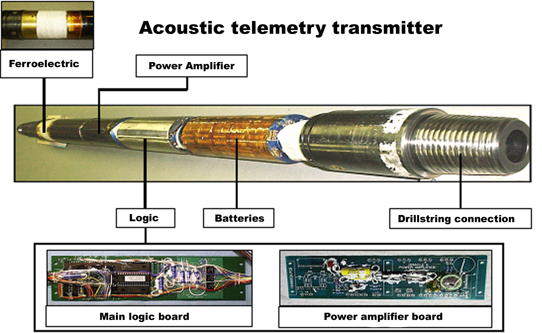
Acoustic telemetry technology uses the well-drilling tubing as the data transmission medium and sound waves as the data carrier. Among the advantages compared to existing techniques: a 10-fold improvement in data rates and no blocking of the fluid flow path.
Doug Drumheller, Sandia project lead for the technology, says that although the acoustic telemetry concept has been around for more than 50 years, the industry’s trial-and-error approach to solving the technical problems involved led nowhere.
“We applied some science to the problem,” Drumheller says. “We approached the problem carefully over a long period of time.”
He praised Extreme Engineering’s contribution to the effort. “They are licensees of our technology,” he notes. “They’ve jumped into this field with both feet. They’ve contributed to the design of hardware, the intellectual property, and the field-testing of the prototype devices. It’s rare to find a company that steps up to the tasks as well as Extreme [Engineering].”
LEAMS (Low Emissions Atmospheric Metering Separator)
The Low Emissions Atmospheric Metering Separator is a family of atmospheric geothermal separators used in the development of geothermal power. The primary function of the LEAMS is to safely contain and clean the atmospheric vented steam of polluting solids, liquids, and noxious gasses. This system is designed to be environmentally friendly, intrinsically safe, and relatively easy to transport, and assemble. LEAMS has a wide operating range and can be used in drilling, well testing, and geothermal power plant start-up.
The LEAMS technology was supported by work done by Allan Sattler, and was developed by Two-Phase Engineering and Research, Inc., Santa Rosa, Calif. Most fabrication was accomplished by Drill Cool Systems, Inc., Bakersfield, Calif. Sattler led Sandia/DOE support of the project. He provided field and instrumentation support for a separator field test at a large geothermal well in California. He consulted, collaborated, and was in constant contact with the designer and fabricator, especially during the design and fabrication phases of most LEAMS units. He and his Sandia colleagues also provided much of the documentation for the project.
“I am delighted that the talent, creativity, innovation, and competency of these two firms was formally recognized, and I am honored to be associated with them and the technology developed,” says Sattler. “It provides a critical new capability to the entire geothermal industry.”
MEMS-Based Adaptive Optics Phoropter
Sandians Steve Eisenbies and Steve Haney contributed to the opto-mechanical design and integration of a compact, transportable adaptive optics system that improves upon traditional devices currently used in optometrists’ offices. In addition to determining correction needed for near-sightedness or far-sightedness and astigmatism, it also determines corrections needed for high-order aberrations that can interfere with night vision and can provide a preview of that correction to a patient. The effects of aberrations can be compared to distortions seen in a pool due to ripples on the surface. Diminished night vision or a perception of “halos” can sometimes result from aberrations introduced during laser eye surgery.
The Adaptive Optics Phoropter is a system that uses MEMS-based deformable mirror technology to correct wavefront aberrations in the eye. It combines technologies from astronomy and micromachining to advance the study and treatment of retinal diseases. Applications for the tool include generation of improved prescriptions for custom contact lenses or laser eye surgery, as well as high-resolution retinal imaging. The award is shared by LLNL, which led the project, Sandia, the University of Rochester, Wavefront Sciences, Boston Micromachines Corp., and Bausch & Lomb.
ETO: Mitigating electrical network problems
Lightning strikes, equipment failures, or other anomalies in electric-powered transmission systems can cause brown-outs or even network failures. But a fast-response semiconductor device developed under the direction of Stan Atcitty allows a utility to rapidly convert energy stored in a DC device into AC power and minimize the negative effects of such interruptions on electrical devices.
Under the auspices of the DOE Energy Storage Systems Program, Atcitty led researchers at Virginia Tech in Blacksburg, Va, in the development of the advanced semiconductor unit. Called an ETO (emitter turn-off thyristor), the three-terminal semiconductor device is similar to a MOSFET but capable of switching greater power at high frequencies.
The ETO, rated at 4000A and 4500V, can switch power at 1-3 kHz.
“This component could become a critical part of inverters, motor controllers, and many other power electronics systems that require medium voltage and high current switches,” says Atcitty.
Another possible use for the device is in the US Navy’s All-Electric Ship Initiative. Says Atcitty, “Once you mention an all-electric ship, you need high-power switching devices like the ETO to manage power flow on a ship.”
The DOE program that supported the ETO development is managed at Sandia by Energy and Transportation Security Center 6200.
The ETO R&D 100 application was a joint entry with Solitronics (a Blacksburg small business marketing the ETO), Virginia Tech (ETO inventor), Sandia (which supported the development of the ETO from a concept to an actual product suitable for utility energy storage applications), and the American Competitiveness Institute in Philadelphia (which assisted the team with manufacturing engineering and prototype production of the device).
Isolated Cast-in-Place Microvalves
Brian Kirby, Tim Shepodd, and David Reichmuth were honored for creating microvalves that allow fluids to be shuttled as easily in microfluidic chips as they are on a traditional laboratory benchtop.
For the first time, these valves enable micro-scale systems to combine high-voltage and high-pressure analytical or synthetic techniques. Previous micro-scale systems could not effectively control both electrokinetic and high-pressure hydraulic flow. The new valves are commercially applicable to miniaturization of techniques crucial to drug discovery and evaluation in the pharmaceutical industry, in particular, gradient liquid chromatography analysis. The polymer valves are photopatterned in seconds and moved by pressure to isolate and manipulate fluids in channels. Liquids of interest can be shuttled from one place to another on a chip where measurements can be made, such as identification of a species or its concentration. The results can then be used to select a path for additional analysis. Miniaturization advantages include greater process speeds using minuscule volumes of reagents, which saves money and minimizes impact to the environment.
Sandia has applied for patents both for the recent inventions forming the subject of this award (US patent application serial number 10/610,093, entitled “High-dielectric-strength microvalves,” filed 6/30/2003, US patent application serial number 10/245,224, entitled “Fluorinated silica microchannel surfaces,” filed 9/16/2002) as well as earlier, closely related microvalve inventions (US patent application serial numbers 10/141,906 and 09/695,816, filed 5/8/2002 and 10/24/00 respectively, both entitled “Mobile monolithic polymer elements for flow control in microfluidic devices”). The award recipients are preparing a manuscript on their work, which will be presented at the upcoming MicroTAS 2003 conference in Squaw Valley. Previous Sandia work with microvalves has also been reported in the Journal of Chromatography A (Vol. 979, pp. 147-154, 2002) and Analytical Chemistry (Vol. 74, pp. 4913-4918, 2002).


