ALBUQUERQUE, N.M. — A new process of growing gallium nitride on an etched sapphire substrate, called cantilever epitaxy, may help light up the world with brighter green, blue, and even white semiconductor light emitting diodes (LEDs) — solid-state lighting. The process was developed at the Department of Energy’s Sandia National Laboratories.
Colored LEDs are of interest for displays and even higher-powered lamps like traffic lights. A national initiative is beginning to develop solid-state sources for high-efficiency white lighting.
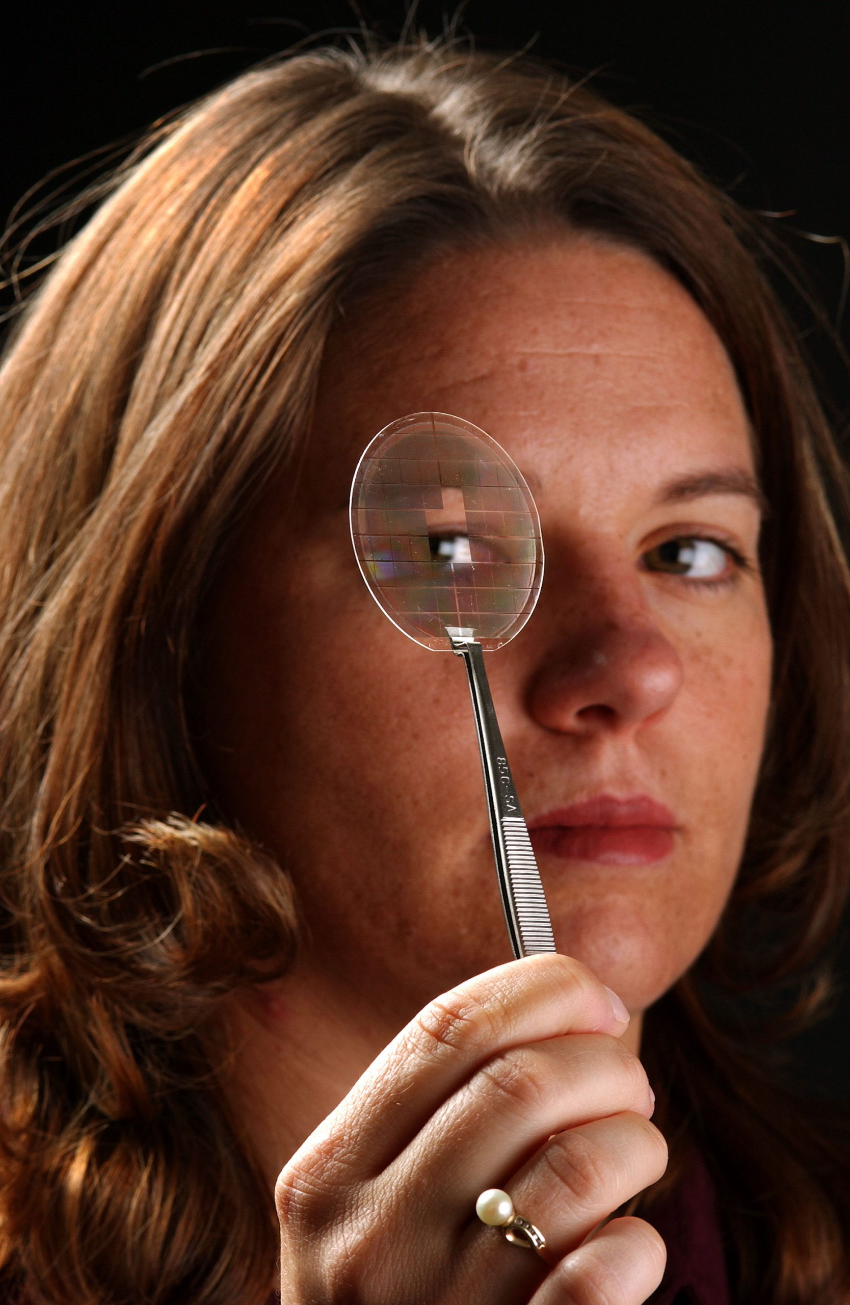
“Our new process eliminates many of the problems that have limited the optical and electronic performances of LEDs previously grown on sapphire/gallium nitride substrates,” says Sandia researcher Carol Ashby.
Over the past several years LEDs have been grown with various combinations of gallium nitride alloys on sapphire substrates. However, the atoms of the two materials do not line up perfectly due to differences in the natural lengths of the bonds in their respective crystal lattices. Regions of imperfections, called dislocations, accommodate this lattice mismatch. These dislocations limit LEDs’ brightness and performance.
The new cantilever epitaxy process developed by a team of Sandia researchers reduces the numbers of dislocations, giving the potential for longer-lived and better performing LEDs. It also means that LEDs grown on the patterned sapphire/gallium nitride substrates can produce brighter, more efficient, green, blue, and white lights than previously accomplished.
Sandia researcher Christine Mitchell notes that a lot of background research has made the improvements possible. Mitchell is investigating cantilever epitaxy as her thesis project for a master’s degree in electrical engineering at the University of New Mexico. She has been involved in just about all stages of the process.
“At Sandia we have four years of experience studying the fundamentals behind gallium nitride growth,” she says. “We took data from basic science work and transitioned it to this.”

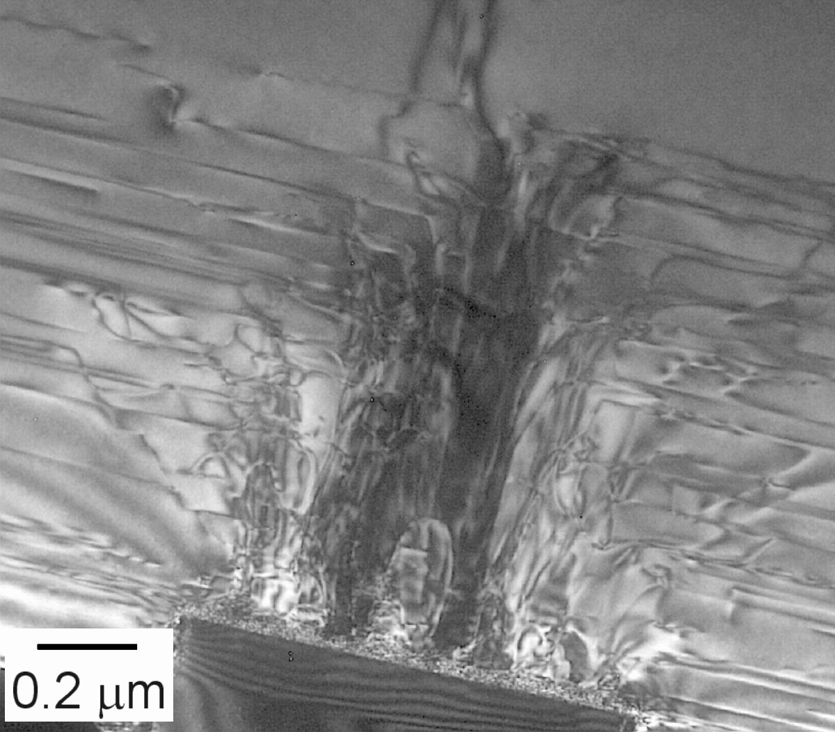
Two methods using transmission electron microscopy (TEM) and scanning electron microscopy (SEM) have been developed to determine the amount of dislocations eliminated through the cantilever epitaxy process. Sandia researcher David Follstaedt slices the material and looks at it “end on” using cross section TEM. (The TEM is a high-voltage microscope that looks through specimens only tenths of microns thick.) These images showed that facets developed early in the cantilever growth process can turn dislocations very effectively when they are grown to full pyramids.
Another TEM imaging orientation is called plan view. Most of the bottom of the sapphire substrate and some of the gallium nitride are removed and the TEM looks through the remaining gallium nitride at the top.
“This is where the rubber meets the road,” Follstaedt says. “This is where you see how many dislocations remain.”
In the other method, called cathodoluminescence, researcher Nancy Missert can check broad areas of the gallium nitride using a SEM equipped with a light detector. This method can survey a whole wafer in half a day and is less labor- and time-intensive than TEM. The dislocations are at points on the surface where the light is not emitted and appear dark. Counting the dark spots gives a measure of the density of dislocations.

Sandia has conducted studies that show good correlation between the two techniques. Both showed that the cantilever epitaxy process reduced the number of dislocations “to an order of a magnitude lower than conventional growth on planar sapphire,” Follstaedt says.
Ashby says that because of the reduction in dislocations, the cantilever epitaxy process shows “great promise for making a superior substrate for light-emitting devices. It also has potential for applications to a wide variety of electronic devices and GaN integrated circuit technology.”
Ashby, Follstaedt, Mitchell, and Jung Han (a former Sandian) have recently been awarded a patent for the cantilever epitaxy process. Cantilever epitaxy substrates have been supplied to LED manufacturers for testing, which should encourage future licensing.
The cantilever epitaxy program at Sandia is part of an internal three-year $6.6 million Laboratory Directed Research and Development (LDRD) Grand Challenge. Funding for the program also comes from a grant from the Department of Energy Office of Building Technologies for a collaborative project with Lumileds Lighting, a joint venture between Agilent Technologies and Phillips Lighting.
Cantilever epitaxy of gallium nitride is of interest for several programs at Sandia, including high-electron-mobility transistors being developed for potential use in miniature synthetic aperture radar systems (SAR) and high-efficiency solid-state lighting being investigated in the Grand Challenge LDRD. Gallium nitride can also be made to emit ultraviolet (UV) light, and compact solid-state UV emitters would be useful for detecting biological and chemical toxins for homeland security.
Cantilevers, posts, and pyramids: How the new process works
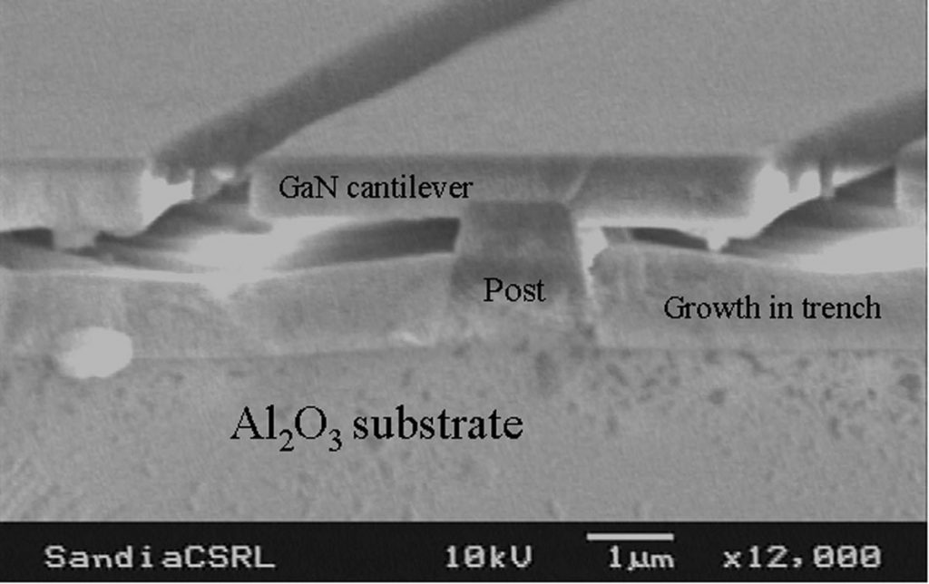
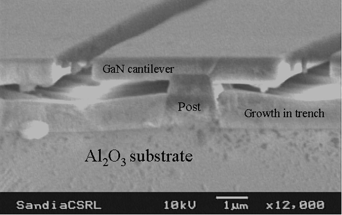
The cantilever epitaxy process, done at the micron level, involves two major steps. First, narrow supports are formed by etching the sapphire substrate using plasma-assisted etching. A multiple-layer photoresist mask is used to define the features to develop a post/trench striped pattern on the substrate. A gallium nitride nucleation layer is then grown on the sapphire posts at a temperature of 500-600 °C. This nucleation layer helps bridge the crystal-lattice difference between the gallium nitride and the sapphire. The growth then proceeds with steps at 1050 °C and then decreased to 950 °C.
“At this point a very key thing happens,” says Daniel Koleske, who is involved in the gallium nitride growth process. “The gallium nitride grows mostly upward, forming natural pyramids that reflect the crystal symmetry of gallium nitride.”
The next step is the coalescence. The temperature is increased to 1100 °C, and the pyramids grow out laterally at a rate faster than they grow vertically. This produces free-hanging cantilevers over the trenches between adjacent posts.
The cantilevers first grow from adjacent posts and meet over the middle of the trench. They then grow together, producing a continuous smooth surface held up by the narrow supports. The areas over the supports have very few dislocations when complete pyramids are formed during the 950 °C growth step. When dislocations growing up from the post surface encounter the angled walls of the pyramids, they are turned from vertical to horizontal so they don’t reach the surface as the material continues to grow thicker.
There are some dislocations where two cantilevers grow together (the coalescence front), but almost no dislocations in the cantilever regions between the posts and the coalescence front. The final result is a continuous smooth surface area with greatly reduced numbers of dislocations. This surface can then be used like a regular gallium nitride substrate to grow LEDs and other devices on top.
Sandia Technical Contact: David Follstaedt, dmfolls@sandia.gov, (505) 844-2102


