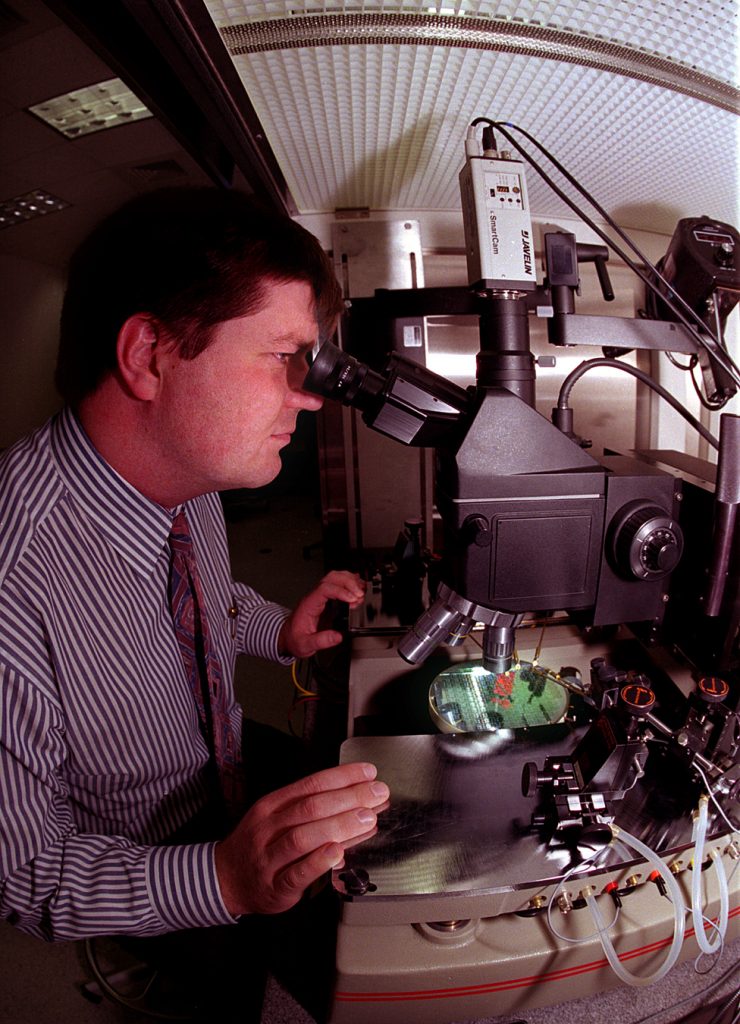
Download 150dpi JPEG image, ‘MEM.jpg’, 1.1MB
ALBUQUERQUE, NM — Within the next few years, your watch, television, and computer may all contain microelectromechanical systems (MEMS), micron-size machines being developed at Sandia National Laboratories, a Department of Energy national security lab.
Jim Smith, manager of Sandia National Laboratories Intelligent Micromachine Department, together with Trey Roessig, Al Pisano, and Roger Howe from the University of California at Berkeley, have built a MEMS prototype that functions as a clock source. The minuscule machines with moving parts the size of a pollen grain perform the same job as quartz crystals, the traditional technology used in timing devices in all digital electronics.
Roessig and Smith made the first public announcement of the prototype in June at the Solid State Sensor and Actuator Workshop in Hilton Head, S.C.
“We have taken the same technology that is now being used in such devices as sensors in car airbags and applied them to a timing device,” Smith says. “It looks extremely promising.”
Micromachines are made from polysilicon, the same material used in manufacturing integrated circuits, the building blocks of digital electronics. Because of this, the micromachines and integrated circuits can be constructed on one chip.
Systems on a chip
The micromachined clock source, conventional integrated circuits, and other micromachined elements can be built simultaneously to form a complete “systems on a chip,” which if mass produced could yield dramatic reductions in price and increases in reliability, Smith says. Hundreds to thousands can be built on a single silicon wafer. In addition, the cost of manufacturing could be significantly reduced because the need for assembly would be eliminated. Under current production methods, quartz crystal timing devices and integrated circuits are manufactured separately and then assembled. Since the two systems would be on one unit, there would be no need to piece them together, saving a significant cost source.
Systems on a chip, a concept only about three years old, embeds the micromachines in a shallow trench on a silicon wafer. These wafers with the micromechanical devices are then used as the starting material for the conventional complementary metal oxide semiconductor (CMOS) manufacturing process of integrated circuits. The integrated circuits are built on the surface of the wafer, while the MEMS are sealed in the trench.
This technology, which in 1996 won Sandia an R&D 100 award, has already been licensed to industry for use in applications such as computer game joy sticks, automotive stability systems and airbag deployment sensors. With incorporation of a timing device, applications for this technology will continue to grow.
Quartz crystals current clock source
Currently, quartz crystals — precision-cut and polished single-crystal silicon dioxide (a main ingredient of sand and window glass) — serve as the clock source. A piezoelectric material, the crystals expand and change shape when an electric field is applied, storing up electric charge. When no current is administered, the crystals release the charge. Electrical energy sloshes back and forth at a fixed frequency between the crystal and the timing circuit in a feedback loop. This fixed frequency generates timing signals, which allow calculations in digital electronics to occur in synchronized steps. For example, a modern wristwatch contains a quartz oscillator and a circuit that counts the oscillations. Once the correct number of counts is recorded, the display is advanced one second.

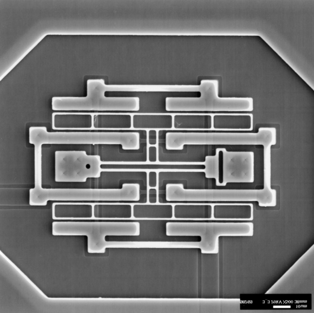
Download 150dpi JPEG image, ‘tuning.jpg’, 473K
MEMS replacement clock source
The MEMS prototype would serve as a replacement clock source. It is different from the quartz crystals because it is excited and sensed electrostatically instead of piezoelectrically. Unlike their quartz counterparts which expand or change shape, these polysilicon resonators physically move in much the same way as a tuning fork vibrates. The prototype also acts somewhat differently from other micromachines used in products currently on the market — such as sensors for pressure and acceleration — that are minute moving gears and pins.
Observed through a high-powered microscope, the MEMS timing device prototype looks exactly like a tiny double-ended tuning fork. It consists of two very fine strings or tines — 10 would fit on a pinhead — anchored in parallel to actuator frames the size of red blood cells. Voltage, set up in a continuous feedback loop (the oscillating effect), is applied through the actuator frames, causing the strings to move back and forth. Because they are so very small, the MEMS vibrate extremely fast and generate frequencies of about 1 MHz. Although this is a relatively low frequency for a system clock, the prototype oscillator is the first integrated oscillator that operates above the audio range.
The process for building these devices at Sandia appears capable of fabricating integrated oscillators with frequencies above 10 MHz. Despite the high frequencies, these micromachines are producing very low noise — due primarily to the integration of the mechanical structure with electronics and the design of the electronic circuit.
The frequencies provide the constant timing signals necessary for the digital electronics device to operate. Because of the low noise, the signals are constant and not disrupted, resulting in more accuracy.
Micromachines in the shape of a tuning fork serving as oscillators are not new. The uniqueness is putting the MEMS oscillator on the same chip as the integrated circuits.
Collaboration with Berkeley
Smith says his efforts build on work done at the University of California at Berkeley by Howe and Clark Nguyen (now at the University of Michigan).
“They were able to get a few of the tuning fork oscillators to work,” he recalls. “But when they saw the dramatic improvement in manufacturability of devices offered by Sandia’s integrated MEMS process, we soon were collaborating with them. They have the expertise in design, and we have the expertise in manufacturing. It’s a natural match.”
He adds that having the clock source on the same chip as other electronic circuitry is one of the building blocks toward developing complete electromechanical systems in a single monolithic piece of silicon.
“Industry has already shown great interest in Sandia’s ability to use this technology to build accelerometers — sensors that measure acceleration used in airbags — and gyroscopes that sense the rotation of a vehicle. The new ability to use micromachines as timing devices will greatly expand the fields of application for these systems on a chip,” he says.
Technical contact:
Jim Smith, smithjh@sandia.gov, (505) 844-3098
