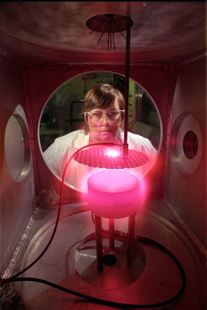
ALBUQUERQUE, N.M. — A glitch in a microchip manufacturing plant can be costly. After hundreds of internal processes have nearly fabricated the next batch of wafers and, say, circuits are plasma-etched to the wrong depth and the defect goes unnoticed, the ruined lot may mean millions of dollars in sales have been delayed or lost.

A sophisticated computer program developed by researchers at the Department of Energy’s Sandia National Laboratories, coupled with a camera and peripheral equipment, should help microchip fabrication companies better monitor the etching process and sharply reduce the number of these large losses.
“It’s to a corporation’s advantage to recognize and correct malfunctions in production as they occur. The possibilities of loss are enormous, running into the millions of dollars,” says Sandia scientist Pam Ward, who with Sandia researchers Joel Stevenson and Michael Smith, developed the technique.
Ward plans a two-year entrepreneurial leave to market the product they created.
The program and machine package will be made available to interested companies “at competitive prices,” according to Ward.
The relatively inexpensive technology also rectifies fabrication errors in the last stages of manufacture of printed circuit boards. An intact, high-end circuit board batch sells for about $100,000.
Says Rick Markle, a senior process engineer at Advanced Micro Devices, a chip fabrication company in Austin, Texas, “From a user’s standpoint, I was floored by the sophistication yet simplicity of the revised software.”
The Sandia program can control up to 64 pieces of equipment, and, once the monitor detects failure, can page help, sound an alarm, do diagnostics, adjust plasma parameters, or replace a part.
The technology was originally developed to aid the US circuit board industry, which was “imploding” from foreign competition during the late 1980s, says Sandia manager Cliff Renschler. To rely upon foreign manufacturers for a key item of America’s defense was a less-than-desirable situation, he notes. Sandia played a part in the successful effort to reverse this trend.
Since printed circuit boards and microchips are both etched by plasmas — hot ionized gases — extension of the monitoring technique from board to chip manufacturing was an obvious progression, says Ward.
The Sandia process uses a camera that spectroscopically analyzes optical emissions from plasmas as they etch printed boards or silicon wafers. While the technique is not new, Sandia’s sophisticated programming allows near-instant analyses of emitted wavelengths to detect if the plasma is misbehaving.
“Plasmas have a fingerprint,” says Ward. “Our tool looks at that fingerprint, then compares it to fingerprints of known failure. The pattern recognition is done by a laptop computer, which is part of the tool.”
“It’s absolutely valid to say that Sandia has delivered by learning what industry needed and we’re excited for ’97,” says Markle of Advanced Micro Devices earlier this year. The company has been working with Sandia on the project since September 1995 as part of a Sematech project, and put the new developmental program in place in December l996. Sematech is an Austin-based consortium of American semiconductor manufacturers.
The problem with plasmas, says Ward, is that “they don’t always behave as they should. Two or three gasses may be involved, and manufacturers hope that everything remains constant, but the mechanisms are temperamental. There may be a leak that allows air to enter and form its own plasma. Or, the flow controllers — electronic valves — may stick, producing the wrong mix, or the pumping speed may be off, or a residue of moisture may be in the system. It all affects how plasma performs.”
In circuit board fabrication, while the technique of monitoring plasmas to etch circuits was well known, the complex program developed at Sandia allows corporations to analyze the process as it occurs and correct a variety of malfunctions before a batch is spoiled.
Curiously, one circuit board problem the technique can’t overcome is what it was originally designed to detect — the moment of complete removal of the epoxy smears that develop near the end of the fabrication process, when epoxy substrates heat, liquefy and flow into circuit holes as they are drilled. According to Ward, “It’s not like removing oil from a surface — epoxy is part of the board’s makeup, and will always emit visual signals that epoxy is present.”
The technique does help the circuit board industry approximate the moment of removal by assuring that the plasma is healthy and working accurately, says Ward.
The smear detection aspect of the technique works better on semiconductor wafers, which consist of a masking material over silicon. “Once the mask material is removed, it’s all gone,” says Ward.
The technology is an outgrowth of work performed in a cooperative research agreement between Sandia and the National Center for Manufacturing Sciences in Ann Arbor, Mich., to improve the manufacture of circuit boards.
Sandia is a multiprogram Department of Energy laboratory, operated by a subsidiary of Lockheed Martin Corp. With main facilities in Albuquerque, N.M., and Livermore, Calif., Sandia has major research and development responsibilities in national security, energy, and environmental technologies and economic competitiveness.
Color photos available
Technical contact:
Pam Ward, now a former Sandian, can be reached at her new company,
Peak Sensors Systems (505) 246-8885
2309 Renard SE, Suite 210
Albuquerque, NM 87106.
