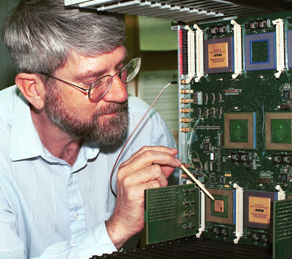
Download 300dpi JPEG image, ‘encrypt.jpg’, 2Mb (Media are welcome to download/publish this image with related news stories.)
ALBUQUERQUE, N.M. — The world’s fastest encryption device, developed at the Department of Energy’s (DOE) Sandia National Laboratories, should soon be protecting data being transmitted from supercomputers, workstations, telephones and video terminals. It encrypts data at more than 6.7 billion bits per second, 10 times faster than any other known encryptor.
“It’s phenomenal,” says Lyndon Pierson, engineer who designed the apparatus. “We have produced a device that has both the security and bandwidth necessary for the protection of all types of digitized information — voice, audio, video, cell phone conversations, radio and television transmissions, banking and credit card information and general purpose computer data — at speeds previously unimagined.”
The Sandia work resulted in an unclassified encryptor chip, called the “SNL Data Encryption Standard (DES) Application Specific Integrated Circuit (ASIC).” It is the fastest known implementation of the DES algorithm, a mathematical transformation commonly used to protect data by cryptographic means.
The device consists of 16 sets of 16,000 transistors on an integrated circuit chip the size of a dime. Data, broken down into single bits of information in 64-bit units, are pipelined through the transistors, where a computationally intense algorithm scrambles the information so that it becomes incomprehensible to anyone who does not have the cryptographic key.
Pierson says it’s the 16 sets of transistors that produce the speed of the new encryption device.
“Other encryptors have one set of approximately 16,000 transistors and the data bits are cycled through the transistors 16 times,” he says. “In this device the information bits flow through the 16 sets of transistors in clocked cycles where they are encrypted.”
Pipelining increases the device’s speed by dividing the algorithm into 16 equally sized blocks where the transistors are located and latching information at the block boundaries. The signals have just enough time to process through each block between clock cycles, thereby maximizing the operational frequency.
Another feature making the DES ASIC unique is that it can process data differently on each clock cycle. For example, the device may encrypt data with one key on one clock cycle, decrypt new data with a different key on the next clock cycle, bypass the algorithm and not be encrypted on the following clock, and then encrypt data with another independent key on the fourth clock cycle. Having this ability gives the device a high degree of key and function agility not found in any other encryptor/decryptor.
The DES ASIC serves at the transmitting end as an encryptor, which scrambles information, and at the receiver end as a decryptor, which unscrambles it. Large supercomputers, like the ones at Sandia, might have four encryption chips, while a personal computer, which operates at much lower speeds, would have only one. The device has the flexibility to encrypt and decrypt rapidly or slowly depending on the capability of the information source or receiver.
While the device has been tested at encryption speeds of 6.7 billion bits per second, it can actually operate much faster. The 6.7 billion bits per second was the limit of the tester used for verification. Simulations predict that the DES ASIC can operate at 9.28 billion bits per second. And parallel operations of these devices — having more than one chip operating at one time — enables encryption at even higher rates.
Fast encryption and decryption are particularly important when sending or receiving large amounts of secure data through various methods that might include telephone wires, fiber optics, or satellites.
Currently, the fastest commercial encryptor operates at 0.15 billion bits per second, which means long waits for large amounts of data to move from supercomputers to visualization stations, for example. The DES ASIC is the first encryption device fast enough to secure the standard 2.5 Gb/s and 10 Gb/s communication channels now being used to carry the ever increasing data traffic for Internet commerce. The device will enable the manufacture of encryption systems to satisfy these high-speed communication requirements.
Pierson says design work of the DES ASIC was done in six to eight months in 1997. Over the next year, a team of seven refined it and put it into the integrated chip form. The integrated circuit was then designed, fabricated, and tested in Sandia’s Microelectronics Development Laboratory.
During the two years since the DES ASIC was conceptualized, the National Security Agency saw merit in the work and commissioned GTE to build a classified version that will be installed in high-speed DOE and DoD classified computer networks in the near future.
“We achieved the primary objective of our work — influence the design of a computer encryptor for classified use,” Pierson says. “We facilitated rapid maturation of a much-needed product to meet DOE requirements.”
The techniques used in the design of the DES ASIC can accommodate both the DES algorithm, which has been a federal standard since 1977 for the protection of sensitive yet unclassified data, and new stronger encryption algorithms, such as the “Advanced Encryption Standard” (AES), expected to be adopted as a standard soon. Because of this, Pierson anticipates that in the next few years, even faster variations of this encryptor chip, performing DES and/or AES, will be found in many commercial applications and will be used, for example, to protect data being transmitted from unclassified supercomputers, Internet connections, cell phones, radio, and television.
“This technology will become increasingly necessary in order to meet the never-ending demand for increased communication speed and data protection in coming years,” Pierson says. “The need for protection of data will dramatically increase as Internet-based trade proliferates.”
