Download 300dpi JPEG image, ‘tra_overview.jpg’, 176K (Media are welcome to download/publish this image with related news stories.)
ALBUQUERQUE, N.M. — Just as a movie theater’s “coming attractions” help viewers choose movies they may want to see, preview images — computer -generated — of possible micromachines help designers choose the device they want fully fabricated.
The need for previewing is particularly important because microdesigns for telecommunications, inkjet printing, and medical and auto safety devices — to name just a few — are fighting for dominance in new, still unestablished fields.
So it is disheartening for designers to learn — after months of work designing a prototype, followed by the time and cost of fabricating it — that a brainchild needs further modifications before it can be marketed as a workable device.
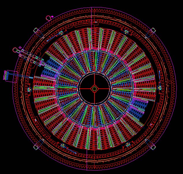
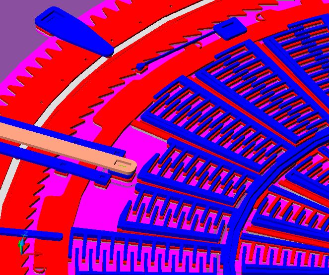
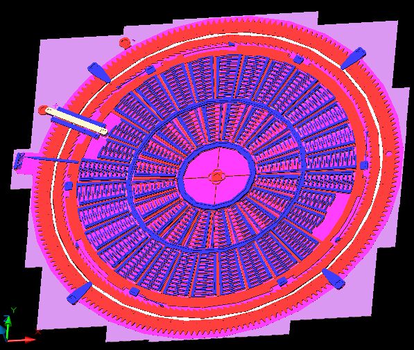
To make life easier for designers, Sandia National Laboratories researchers Vic Yarberry and Craig Jorgensen have crafted 2-D and 3-D modeling programs.

Two-dimensional modeling shows the flat-plane cross sections of devices as they would look if fabricated. The 3-D version allows designers to twirl their virtual microdevices like airplane parts modeled in the macroworld, the still-imaginary part viewed from any perspective. Unworkable portions of the design can be modified or eliminated before — not after — fabrication work is paid for at the foundry. Sandia is a US Department of Energy laboratory.
“It’s not intuitive how the layers interact,” says Jorgensen. “MEMS [microelectromechanical systems] are wonderful in that they come out thousands at a time, all in one piece with no assembly necessary, but there’s nothing about fabricating them that is simple. You’re building patterned layers on top of other patterned layers, which can create a complex 3-D geometry.”

“It’s not easy for former macro–world designers to combine 2–D mask geometry with newly learned information about the MEMS fabrication process itself,” says Yarberry, “and, on the first try, to create functional 3–D structures.”
Glitches occur because most researchers who design multilayered microdevices find it difficult to visualize how the micron–sized features of the etched layers fit together.
The simulation process does take time. A simple microdevice can be simulated in seconds; a complicated one can take hours. Still, waiting for a computer to complete its complex modeling beats waiting months to find out what modifications one should have made.
Sandia’s Marc Polosky, who designs safety components in weapons systems, says the 2-D cross-sectioner enables him to visualize the effect of cuts in different thin film layers.
Put simply, he says, “If you’re makng a gear on a pin joint, the program helps make sure you’re not designing a gear that’s rigidily fixed to the substrate and can’t move.”
While the 2-D program is a valuable design tool that should help new designers get up to speed faster, Polosky says, the 3-D modeler has potential of going to the next step — kinematic modeling — that will demonstrate these devices performing in environments.
Two papers by Yarberry and Jorgensen on their modeling work were selected for presentation at the Fourth International Conference on Modeling and Simulation of Microsystems, held this past spring at Hilton Head Island. The conference is probably the largest and most prestigious in providing an interdisciplinary forum for modeling, simulation, and scientific computing in the microelectronic, semiconductor, sensors, materials, and biotechnology fields.
Sandia Technical contacts:
Jay Jakubczak, jayj@sandia.gov, (505) 844-9196
Vic Yarberry, vryarbe@sandia.gov, (505) 844-9322


