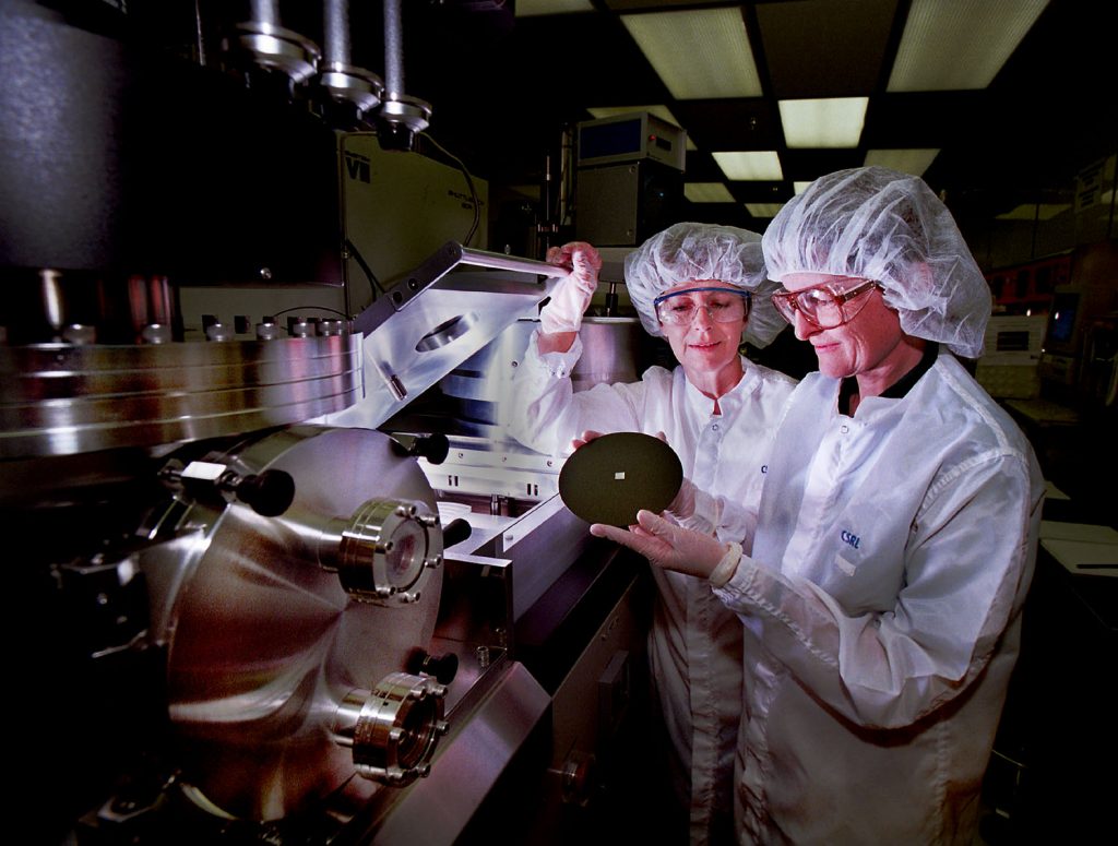
Download 300dpi JPEG image, ‘lab.jpg’, 273K (Media are welcome to download/publish this image with related news stories.)
ALBUQUERQUE, N.M. — You could say these chips have ridges.
Researchers at the Department of Energy’s Sandia National Laboratories have created a new microchip processing technique that creates raised, microscopic canals on chips, through which liquids or gases can flow from one chip feature to another.
Such canals are useful for emerging families of minuscule gadgets called “microfluidic” devices that make use of the chemical properties of liquids or gases and the electrical properties of semiconductors on a single chip or among nearby chips.
Better detectors for airborne toxins, rapid DNA analyzers for crime-scene investigators, and new pharmaceutical testers for drug development are among the possible future uses for inexpensive microfluidic devices.
The technique’s compatibility with standard semiconductor batch-processing tools should allow future microfluidic devices to be made quickly and cheaply in a microchip factory, says co-developer Carolyn Matzke of Sandia’s Compound Semiconductor Research Laboratory.

Download 300dpi JPEG image, ‘csrl_A.jpg’, 168K (Media are welcome to download/publish this image with related news stories.)
Microscopic canals on chips
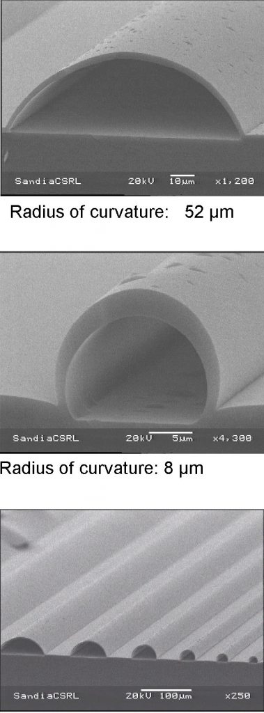
Using the patented new technique, the researchers have created raised, hemispherical canals on silicon, glass, and quartz surfaces that are 8 to 100 microns in diameter. They’ve also made canals with tight turns, creating hairpin curvatures with radii as small as 8 microns.
To get an idea how small the canals are, imagine slicing a human hair in half lengthwise. The remaining half-strand of hair might fit snugly in the largest of the canals. The smallest of the canals are less than one-tenth that size, so small you would need a microscope to see them.
The canals can be small enough and curvy enough that some liquids or gases pass easily through them and others pass more slowly. This ability to distinguish among fluidic materials is useful for chemical-separation applications, the most common use of microfluidic devices.
The traditional method for creating canals on chips — called “trench and seal” — involves the careful joining of two pre-trenched wafers. But the intense heat required for bonding — up to 1,000°C — can damage other chip features, and the care necessary to remove contaminant particles from the two halves increases the difficulty and cost of manufacturing.
To make the Sandia canals, the researchers pattern a thin layer of photoresist on the wafer’s surface using a conventional photo mask and light, then develop away areas of the photoresist exposed to the light, leaving a network of photoresist ridges on the wafer’s surface that eventually becomes the canals’ interiors.
Next they heat the wafer to a relatively low 100°C for about 20 seconds, which causes the square-edged ridges to slump into a hemispherical shape. A 2-micron-thick film of silicon oxynitride is deposited over the rounded photoresist, and the entire wafer is soaked in an acetone bath until the remaining photoresist is dissolved, leaving hollow tunnels on the wafer’s surface.
The technique is 10 to 100 times faster than trench-and-seal techniques, says co-developer Carol Ashby, and the resulting tunnels are virtually indestructible.
A range of new applications
Ultimately the technique could bring better detectors for air or water pollutants or for chem-bio warfare agents (one goal of Sandia’s “microchem-lab-on-a-chip” development program), because the low-temperature processing might allow fragile organic materials with useful properties to be integrated into the microfluidic devices, says Terry Michalske of Sandia’s Biomolecular Materials and Interfaces Department.
Canal networks also could be used to separate and analyze DNA for crime-scene forensics, or proteins for biomedical research that seeks to understand human responses to toxins or diseases. In the pharmaceutical industry, such devices could help develop better drugs by analyzing responses of hundreds of proteins simultaneously.
“You could envision an elaborate microfluidic network on a chip that sorts, detects, and identifies individual chemicals or proteins,” Michalske says.
Microfluidic channels might be embedded with electronic controls, micromachines, or novel materials to create an electrokinetic pump or tiny valves or filters. They could deliver cooling fluids to hot spots on today’s tightly packed microchips. Or they might help create on-chip insulators that reduce electrical cross-talk.
“We’re now just beginning to think about all the potential applications for microfluidic devices using this technique,” he says.
The Sandia researchers are now working to integrate the new canals with other microelectronic and micromechanical features.
