Download 300dpi JPEG image, ‘chamber2.jpg’, 372K (Media are welcome to download/publish this image with related news stories.)
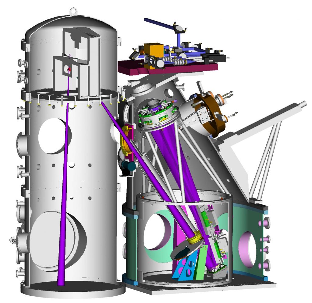
LIVERMORE, Calif. — Industry and government officials today announced completion of the first full-scale prototype machine for making computer chips using extreme ultraviolet (EUV) light, a breakthrough that will lead to microprocessors that are tens of times faster than today’s most powerful chips and create memory chips with similar increases in storage capacity.
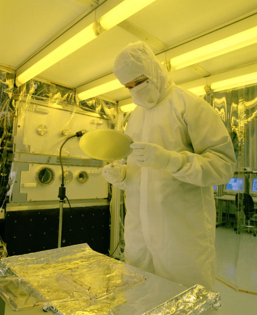
Akin to photography, lithography is used to print circuits onto microchips. EUV lithography was developed because the current chip-printing technology is expected to reach its physical limits in the next few years.
Current lithography technology is expected to allow manufacturers to eventually print circuits as small as 0.1 micron in width, or 1/1,000th the width of a human hair. EUV lithography technology is being developed to allow semiconductor manufacturers to print circuit lines well below 0.1 micron — down to at least 0.03 microns, extending the current pace of semiconductor innovation at least through the end of this decade.
“The completion of the prototype machine marks a major milestone for the program, since we have proven that EUV lithography works,” said Chuck Gwyn, program manager of the EUV Limited Liability Company (LLC). “Our next step is to transfer the technology to lithography equipment manufacturers to develop beta and production tools.”

Download 300dpi JPEG image, ‘euvl_01_033001.gif’, 456K (Media are welcome to download/publish this image with related news stories.)
Processors built using EUV technology are expected to reach speeds of up to 10 GHz in 2005-2006. By comparison, the fastest Pentium 4 processor today is 1.5 GHz.
The prototype machine, called the Engineering Test Stand (ETS), was developed by industry-government collaboration among three U.S. Department of Energy national laboratories and a consortium of semiconductor companies called the EUV LLC. The consortium includes Intel Corporation, Motorola Inc., Advanced Micro Devices Inc., Micron Technology Inc., Infineon Technologies, and International Business Machines.
The three DOE national laboratories, combining EUV research efforts in a Virtual National Laboratory, are Lawrence Berkeley National Laboratory, Lawrence Livermore National Laboratory, and Sandia National Laboratories in California.
Using the EUV LLC, private industry has funded 100 percent of the EUV lithography research through an agreement that spans from 1997 through early 2002.
“The EUVL partnership demonstrates that fundamental science and innovative ideas can be applied toward solutions in both the commercial and public sectors,” said John Gordon, administrator of the DOE’s National Nuclear Security Administration. “These kinds of challenges are exactly the kind of work our national laboratories do best.”
The ETS was assembled at Sandia in Livermore, California. It will be used by LLC partners and lithography tool suppliers during the next year to refine the technology and get it ready to create a prototype commercial machine that meets industry requirements for high-volume chip production. The EUV LLC has developed relationships with more than 40 U.S.-based infrastructure companies to ensure that all of the key components can be attained for commercialization.
About EUV LLC
Intel began substantial funding for EUV research in 1996, and established the EUV LLC in 1997 with Motorola and Advanced Micro Devices. Micron Technology and Infineon Technologies joined the EUV LLC in early 2000; International Business Machines joined in 2001. Rapid technical progress in the EUV LLC program has attracted widespread interest and support for EUV technology, as chip manufacturers and their suppliers recognize that this technology can support multiple process generations and be cost effective for producing all types of semiconductor chips.
Extreme Ultra Violet Lithography (EUVL) Milestone Celebration Background
Virtual National Laboratory contacts:
Gordon Yano, yano1@llnl.gov, (925) 423-3117
