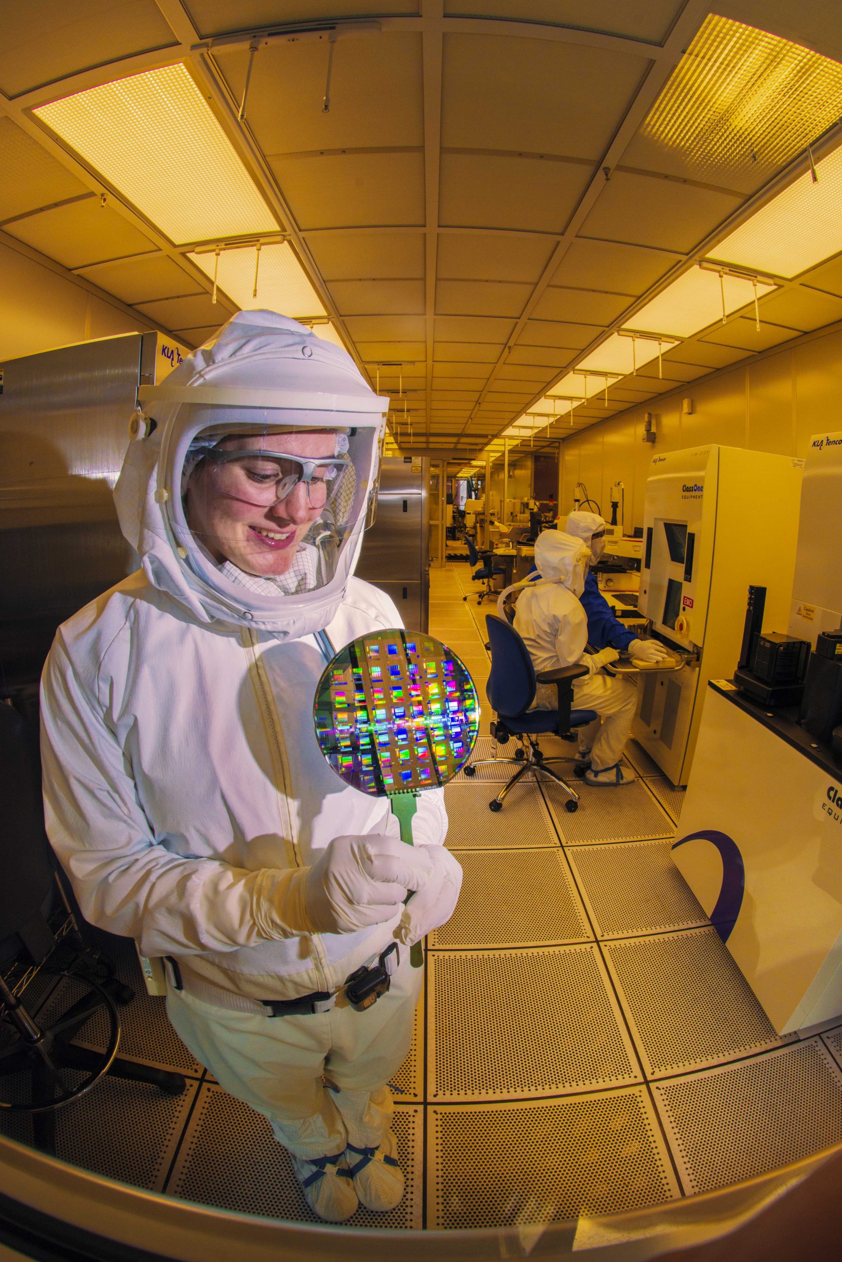
ALBUQUERQUE, N.M. — Sandia National Laboratories has completed phase one of an anticipated three-year upgrade at its plant responsible for making integrated circuits, similar to computer chips. The facility is now fully compatible with industry-standard, 8-inch silicon wafers — thin, round starting materials used for making chips. Previously, Sandia used 6-inch wafers.

Supporting the new size will help sustain production of microsystems for national security applications through 2040. Prototyping and product development activities have already resumed.
“Moving to 8-inch wafers aligns us with industry, which means we have a more sustainable supply of starting materials, tools and service,” said Sandia senior manager Mike Holmes, who is overseeing the process.
Larger wafers are generally more cost-effective than smaller ones because more devices can be made per wafer, Holmes said. That’s why they’ve been widely adopted in industry.
Sandia’s decision, however, was driven by its national security mission. Six years of planning ensured the conversion would not affect production of components needed for national defense. Chips produced at Sandia can be found in the nation’s nuclear stockpile.
Much of the site’s staff have taken on new roles to assist with the upgrade, enabling Sandia to cover 85% of expenses with the facility’s regular operating budget. The conversion has been underway since August 2018.
The fabrication plant is part of Sandia’s Microsystems Engineering, Science and Applications (MESA) complex, which is world-renowned for producing high reliability components that last for decades. It is a world leader in protecting integrated circuits from otherwise damaging radiation.
The complex is also home to a research and development lab that invented the world’s fastest digital X-ray camera, and a microfabrication plant supporting production and research of compound semiconductor devices.
Upgrade modernizes production process
At MESA, the journey from a raw silicon wafer to a finished chip takes hundreds of steps. Many specialized pieces of equipment handle, treat, build on, cut and test manufactured components. Every machine that touches wafers had to be modified or replaced.
This included the implanter, an 8-foot-tall, 19-year-old cube in which electrically charged elements, or ions, are accelerated and embedded into the wafers to tune their chemical and electrical properties. Construction crews had to tear down a wall to get the machine out of the building. Then, they had to raise the ceiling and reinforce the floor for its 10-foot-tall replacement.
Other upgraded systems included equipment that uses light to transfer geometric patterns from stencils to precisely plot the locations of circuits, and chemical-mechanical polishing tools that smooth and flatten surfaces for multi-layer processing.
The tooling upgrade is the first of four steps toward the facility’s conversion. The remaining three steps review and requalify the production line to ensure products made using the new equipment are identical to ones produced by the old equipment.
“Re-establishing the process on 8-inch wafers is extremely challenging,” Holmes said. “We have to tune hundreds of interrelated parameters to get the same end result as before but with different equipment and at a larger scale.”
This process, called requalification, is expected to be finished in 2021.
