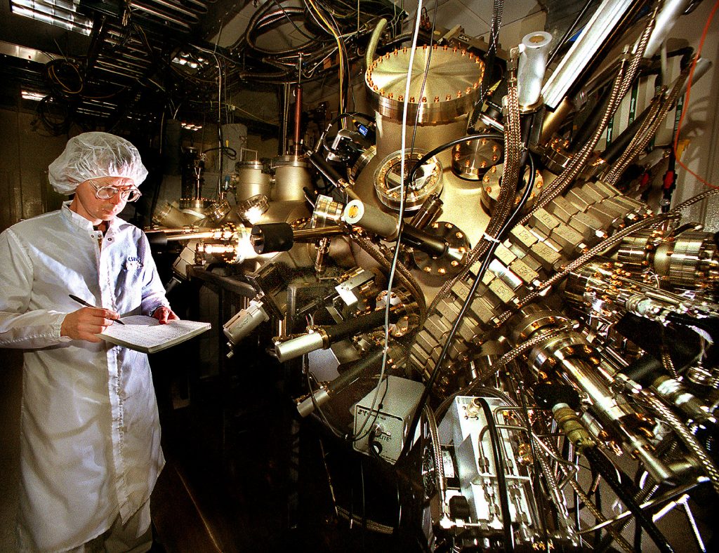
Download 300dpi JPEG image, ‘MBE.jpg’, 1.9Mb (Media are welcome to download/publish this image with related news stories.)
ALBUQUERQUE, N.M. — Researchers at the Department of Energy’s Sandia National Laboratories have developed the first 1.3-micron electrically pumped vertical cavity surface emitting laser (VCSEL) grown on gallium arsenide. It promises to reduce the cost of high-speed fiber optics connections.
Working through a cooperative research and development agreement (CRADA) with Cielo Communications, Inc., Sandia developed the gallium arsenide-based VCSEL, which will be cheaper and easier to build than standard edge emitting lasers used in current high-speed communications.
“This VCSEL will meet the needs of high speed fiber optics connections of the future,” says Peter Esherick, manager of the Compound Semiconductor Materials and Processes Department at Sandia. “We expect there to be great excitement over the device — fueled by the rapid expansion of Internet use and craving for faster Internet access.”
The new 1.3-micron VCSEL is made mostly from stacks of layers of semiconductor materials common in shorter wavelength lasers — aluminum gallium arsenide and gallium arsenide. The Sandia team added to this structure a small amount of the new material, indium gallium arsenide nitride (InGaAsN), which was initially developed by Hitachi of Japan in the mid 1990s. The InGaAsN causes the VCSEL’s operating wavelength to fall into a range that makes it useable in high-speed Internet connections.
Esherick says laboratories around the world have been in a “horserace to be the first with the 1.3-micron VCSEL on gallium arsenide substrates.” Cielo teamed with Sandia through a CRADA last year to research several compound semiconductor alloys in an effort to find the one that achieved the 1.3-micron goal. In May, Sandia researchers came up with a materials combination and materials growth technique that hit the target. The research findings were submitted June 1 to Electronic Letters for publication.
The laser is the light source that transmits information down optical fibers. Two types of semiconductor lasers are used in high-speed data and telecommunications fiber optics — the edge emitter and the VCSEL. In the edge emitter, which has traditionally dominated the semiconductor laser market, photons are emitted out of one edge of the semiconductor wafer after rebounding off mirrors that have been literally cleaved out of the crystalline substrate.
In the VCSEL, laser photons bounce between mirrors grown into the structure and then emit vertically from the wafer surface. VCSELs, which are grown by the thousands on a single wafer, have significant advantages over edge-emitting lasers in the areas of lower manufacturing, packaging, alignment, and testing costs, as well as lower power dissipation and higher reliability.
VCSELs made of combinations of aluminum gallium arsenide and gallium arsenide have been used in the shorter wavelength window of 850 nanometers for local connections. However, because none existed that could work in the 1.3-micron window required for high-speed, long-distance communications, the optical networking industry turned to the more expensive and complicated edge emitting lasers.
Sandia researchers successfully built an edge emitter using InGaAsN early this year, giving them the opportunity to characterize the material’s properties and quality. They now have gone to the next step with development of the first InGaAsN VCSEL.
“The key to making this work was to optimize the material quality of the InGaAsN and to make subtle changes to the rest of the structure,” says John Klem, Sandia researcher working on the VCSEL project. “Once we had the high quality InGaAsN in hand, our extensive experience with shorter wavelength VCSELs allowed us to quickly produce the full 1.3-micron device.”
Mike Cowley, president and CEO of Cielo Communications located in Broomfield, Colo., says the InGaAsN VCSEL is an “extremely exciting announcement for Cielo, Sandia, and the optical networking industry as a whole.”
“VCSEL technology has historically provided the most cost-effective optical link solution for high-bandwidth applications, proven in recent years by their rapid adoption over edge-emitting lasers in the data communications market,” he says. “The significant cost reduction afforded by the 1.3-micron VCSELs will make increased bandwidth more accessible and cost effective for the telecommunications and Internet infrastructure.”
Esherick says in addition to the obvious benefits of 1.3-micron VCSELs for the civilian telecommunication markets, there are equally important benefits for DOE’s defense applications.
“What’s exciting for us is that the 1.3-micron light can be transmitted through silicon — the silicon is transparent at that wavelength,” he says. “The additional flexibility this offers for integrating photonic devices with silicon based microsystems will have significant implications for national security systems.”
