ALBUQUERQUE, N.M. — You can‘t get something for nothing, physicists say, but sometimes a radical innovation can come close.
Researchers at Sandia National Laboratories — exceeding the predictions of a 100-year-old law of physics — have shown that filaments fabricated of tungsten lattices emit remarkably more energy than solid tungsten filaments in certain bands of near-infrared wavelengths when heated.
This greater useful output offers the possibility of a superior energy source to supercharge hybrid electric cars, electric equipment on boats, and industrial waste-heat-driven electrical generators. The lattices’ energy emissions put more energy into wavelengths used by photovoltaic cells that change light into electricity to run engines.
Because near-infrared is the wavelength region closest to visible light, the day may not be distant when tungsten lattice emissions realized at visible wavelengths provide a foundation for more efficient lighting — the first significant change in Edison‘s light bulb since he invented it.
“This is an important and elegant work,” says Cal Tech professor Amnon Yariv of the research achievement. Yariv is a member of the National Academy of Engineering and a leading figure in quantum optics research.
The work has been granted two patents with another pending. Two papers describing the advance have been accepted by the journal Optics Letters. Another will be published by Applied Physics Letters.
Sub-micron-featured lattices — which resemble very tiny garden lattices carefully stacked one atop the other — can be mass-produced cheaply with todays computer-chip technologies.
The lattice itself can be visualized as a construction built of a childs Lincoln Logs. The tungsten “logs” of this experiment have diameters of 0.5 microns separated by distances of 1.5 microns.
The lattices are also known as photonic crystals because of the crystalline regularity of the spacing of their components. At first such crystals were of interest because they could bend specific frequencies of light without loss of energy. This was because the crystal’s channels were constructed of exactly the right dimensions to form a ‘home’ for particular wavebands as they travelled. The innovation of the current method is to use the channels not to bend light but to permit input energy to exit only in the desired frequency bands.

The shadow of Max Planck
The demonstration, led by Sandia physicist Shawn Lin, exceeds in output a well-known law formulated a century ago by Max Planck, one of the founders of modern physics. The equation, called Planck’s Law of Blackbody Cavity Radiation, predicts the maximum emissions expected at any wavelength from ideal solids.
The somewhat startling Sandia results exceeded these predictions by four to 10 times at near-infrared frequencies, says Lin.
In terms of electrical output, for the Sandia lattice heated in a vacuum to 1,250 degrees C — the typical operating temperature of a thermal photovoltaic generator — a conversion efficiency of 34 percent was calculated, three times the performance of an ideal blackbody radiator, predicted to be 11 percent.
Electrical power density was calculated to be approximately 14 watt/cm squared, rather than three watt/cm squared expected from an ideal blackbody radiator.
No deterioration of the tungsten lattice was observed, although long-term tests have yet to be run.
Cat vs. supercat
Lin says his group’s work does not break Planck’s law but only modifies it by demonstrating the creation of a new class of emitters.
“To compare the amounts of emissions from a solid and a photonic lattice is like comparing a dog and a cat — or, a cat and a super cat,” he says.
A photonic lattice apparently subjects energies passing through its links and cavities to more complex photon-tungsten interactions than Planck dreamt of when he derived his system that successfully predicted the output energies of simple heated solids. And a lattices output is larger than a solid’s only in the frequency bands the lattices inner dimensions permit energy to emerge in.
Still, says Kazuaki Sakoda of Japan’s Nanomaterials Laboratory at the National Institute for Materials Science, “One of the most important issues in contemporary optics is the modification of the nature of the radiation field and its interaction with matter. [Lin’s] recent work clearly demonstrates that even Planck’s law — the starting point of the era of quantum mechanics [used to predict these interactions] — can be modified. To my knowledge, [Lin’s papers] are the first experimental report on this matter.”
Sakodas book, Optical Properties of Photonic Crystals, was published by Springer Verlag, Berlin, 2001.
Theoretically, there are still unresolved questions as to how the process works without contradicting other physical laws.
Nevertheless, MIT physics professor John Joannopoulus in response to a question from a Sandia interviewer had high praise for the work. “It is definitely not a — how did you put it — ‘a small step forward,’ it’s really a leap forward. It is a very clever experiment that’s completely believable … I think its an exciting experiment, very carefully done, and theres some really interesting new science here. Joannopoulus is a pioneer in photonic lattices and wrote the first book on the field.
The scientist at rest
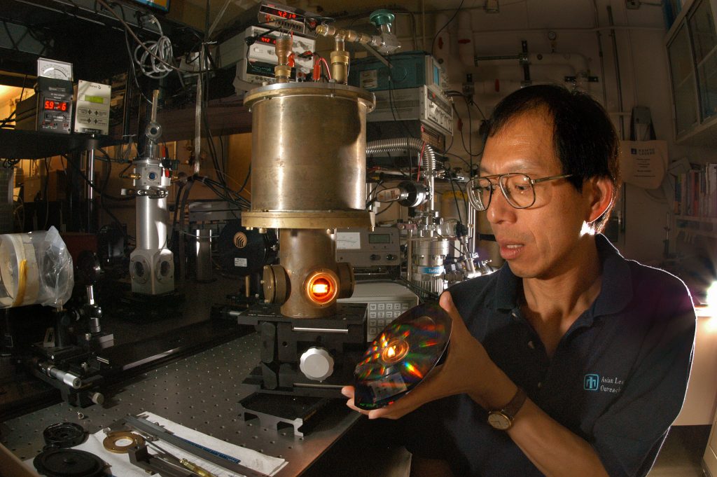
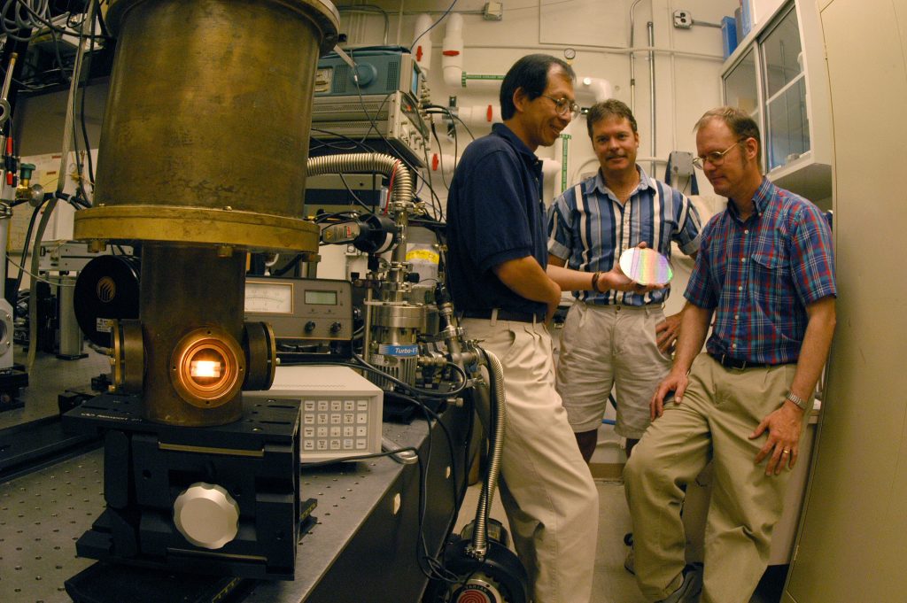
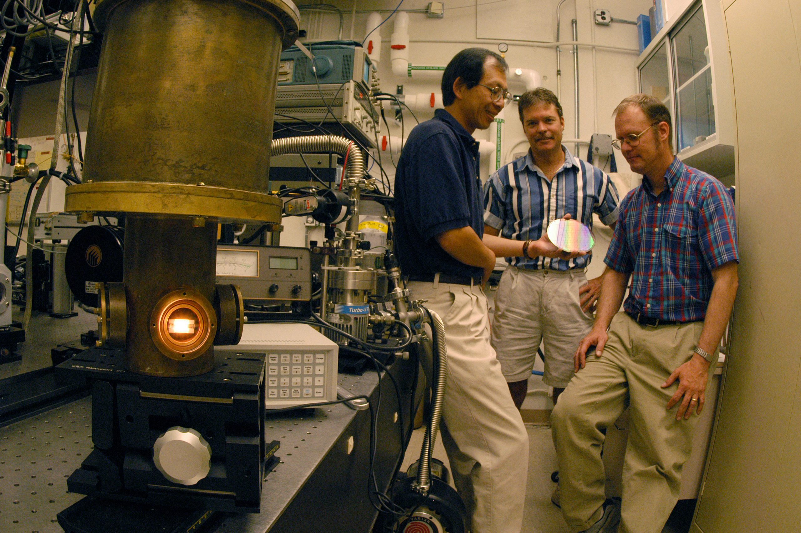
Standing in his equipment-cluttered laboratory, Shawn Lin grins happily among the vandalized wreckage of a number of ordinary light bulbs from K-Mart. His team pirates the bulbs’ screw-in bases and glass filament supports for use as cheap, pre-made connectors and supports for the iridescent slivers of photonic lattice his team substitutes for common filaments of solid tungsten.
“Look!” Shawn says with obvious anticipation, and flips a switch connected to where the reconstituted filament sits in a vacuum chamber.
In its little chamber, like a kind of witches’ Sabbath for light bulbs, the bulb, though formerly dead, now glows again, but with a distinctly yellow light. The lattice filament, powered by only two watts, and with most of its output keyed to the infrared range at 1.5 to 2 microns, has enough of a tail into the visible spectrum for the lattice to glow. “We are that far along!” Lin says with satisfaction.
If these results at 1.5 microns can be extended to the visible spectrum, ramifications of this work may help form the next generation of lighting after the currently more mature LED technology.
Possible applications
The increased amount of usable energy available from lattices (also known as photonic crystals) at specific frequencies is important to engineers dealing with electricity-driven engines.
A photonic lattice absorbing energies from a power plant generator’s excess heat could release it at higher frequencies readily absorbable by the photovoltaic cell that powers electricity-driven engines.
While such engines — best known in the form of electric-powered cars “ exist, their efficiencies have been much lower than hoped because their receivers cannot absorb incoming energies across the wide spectrum of infrared radiation generated as unwanted heat but only from limited bands within the broad range. Here, the lattice could serve as a kind of funnel, forcing the heat radiation into predetermined frequency bands. When placed between the generator — be it solar, dynamo, or fire — and receiver, the metallic photonic lattice can be engineered to absorb energies, become thermally excited, and release them in only a few frequency bands.
While some energy is lost in this process, it makes available energies from frequencies previously unusable.
Visit the past
A year ago (Nature,, May 2, 2002), Lin’s team showed that a tungsten lattice could gather absorbed energies at shorter wavelengths than ordinary tungsten could. Now, Lin with colleagues Jim Fleming, Jim Moreno (ret.), and Ihab El-Kady show actual emissions. The emission measurements were performed with the technical assistance of Jim Bur and Jonathan Rivera. Part of the earlier simulation of tungsten lattice’s optical properties was done at Iowa State University/Ames National Laboratory, in work led by Professor Kai Ming Ho.
The current use of tiny lattices to emanate energy in designated wave bands is a conceptual jump from their earliest appearances over a decade ago, when it was thought their major function would be to bend light without loss for telecommunications. Such lattices were built from semiconductor materials. In the case discussed here, semiconductor materials are used to form a lattice mold into which tungsten is introduced. The semiconductor material is then etched away, resulting in a thin tungsten photonic crystal sample about five micrometers thick.


