ALBUQUERQUE, N.M. — Nuclear reactions are fast. Really fast. Faster than billionths of a second. Your best shot at catching one is with a high-speed X-ray camera that can only be obtained from the Department of Energy’s Sandia National Laboratories. But these cameras could soon become more widely available.

Sandia has partnered with Albuquerque-based startup Advanced hCMOS Systems (pronounced “H C moss”) to commercialize ultrafast imaging technology invented at the Labs and used extensively in fusion research. If successful, the collaboration could move the world more quickly to limitless clean energy by accelerating such research, while potentially impacting many other research and development areas.
“A perfect example is glass research,” said Liam Claus, cofounder of Advanced hCMOS Systems. “The Gorilla Glass that’s in your iPhone so it doesn’t shatter every time it slips out of your hand — there’s a ton of materials science that’s gone into that. They need to understand how it fractures, and glass fractures can propagate at extremely high speeds.”
Claus and his fellow co-founders Marcos Sanchez and Matthew Dayton say they plan to make the cameras available to new markets, including organizations developing other advanced materials, studying astrophysics or designing lasers, all of which could benefit from high-speed imaging, they said.
“Liam’s dream is to see one of these in every university physics lab,” Sanchez said.
Ongoing collaboration lays groundwork for redesigning cameras
Sandia issued its first commercial license for the ultrafast X-ray imager — the fastest multiframe digital X-ray camera in the world — to the company in July 2022. The following month, Sandia and the startup began a one-year collaboration to develop a road map for redesigning the sensors for new applications.
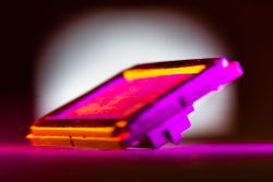
As part of the collaboration, Sandia is testing how well its sensors capture and amplify forms of light besides X-rays, such as visible light. The team evaluates images pixel by pixel for consistency.
“It’s a success so far,” said engineer Rex Kay, Sandia’s lead on the collaboration. “We’ve been testing our old devices in this new mode of operation and were able to demonstrate that they do actually exhibit gain in the right region that we’re looking for in this project.”
This ongoing project is funded by the TRGR Technology Readiness Initiative, formerly the Technology Readiness Gross Receipts Tax Credit program, a partnership between the state of New Mexico, Sandia and Los Alamos National Laboratory. The program helps New Mexico companies grow, strengthening the local economy, by funding projects that mature technology so it can be marketed.
Demand is high for Sandia camera tech
Sandia’s decision to commercialize the technology comes at a time when demand for the sensors is pushing labs’ limit to produce them.

Camera sensors built at Sandia’s Microsystems Engineering, Science and Applications Complex can be found at major research facilities such as the National Ignition Facility at Lawrence Livermore National Laboratory in California, which achieved fusion ignition in 2022, the OMEGA laser at the University of Rochester in New York and Sandia’s own Z Pulsed Power Facility.
“The demand for product is many dozens per year” in addition to service calls and requests for replacement parts, said Tony Colombo, Sandia’s manager over camera production.
To put that demand into context, each batch Sandia produces, usually consisting of around 20 sensors, takes six to nine months to process. Much of the time-intensive work takes place at a semiconductor fab in Sandia’s MESA complex, with some steps outsourced to private companies. It’s possible to start multiple batches throughout the year, but the time it takes to finish them depends on the availability of Sandia’s contracted manufacturers and machinery at the fab. MESA’s primary purpose is to produce microelectronics for the U.S. nuclear stockpile, while serving as a research and development facility for a host of other projects.
After the sensors are completed, they are integrated into hardware, usually built by the customer, to turn them into functional cameras.
“If all the production and ordering parts could be taken over by a small company, Sandia as a federally funded research and development center would go back to its primary core competency, which is research and development of new, advanced, cutting-edge capabilities,” Colombo said, which includes building variations of the cameras with new features and better performance.
Small startup has big plans for speedy sensors
Claus said his company will use licensed Sandia patents to create their own product line of ultra-high-speed cameras. “We offer technical engineering services, whether it’s consultation, whether it’s design or whether it’s manufacturing — for the existing users and existing technology that was developed and manufactured at Sandia,” he said.

Sanchez and Claus are both former Sandia employees. The pair were granted leave in 2021 to start Advanced hCMOS Systems through a program at the Labs called Entrepreneurial Separation for Technology Transfer. Through the program, employees are guaranteed reinstatement if they choose to return within two years. Dayton was formerly employed at Lawrence Livermore National Laboratory.
Sandia is mandated by the DOE to move its technology to the marketplace for the benefit of the U.S. economy. Given the Labs’ national security focus, government is the primary customer for many licensees, but Sandia technologies also find use in the industrial and consumer markets. Sandia issues licenses to companies ranging in size from startups to multinationals.
“That’s a win for the (DOE) complex overall because that technology then gets fed right back into the laboratory at a benefit, whether that be time, cost or quality,” Sanchez said.