A device like a photonic crystal, but smaller and tunable
ALBUQUERQUE, N.M. — Gems are known for the beauty of the light that passes through them. But it is the fixed atomic arrangements of these crystals that determine which light frequencies are permitted passage.

Now a Sandia-led team has created a plasmonic, or plasma-containing, crystal that is tunable. The effect is achieved by adjusting a voltage applied to the plasma, making the crystal agile in transmitting terahertz light at varying frequencies. This could increase the bandwidth of high-speed communication networks and generally enhance high-speed electronics.
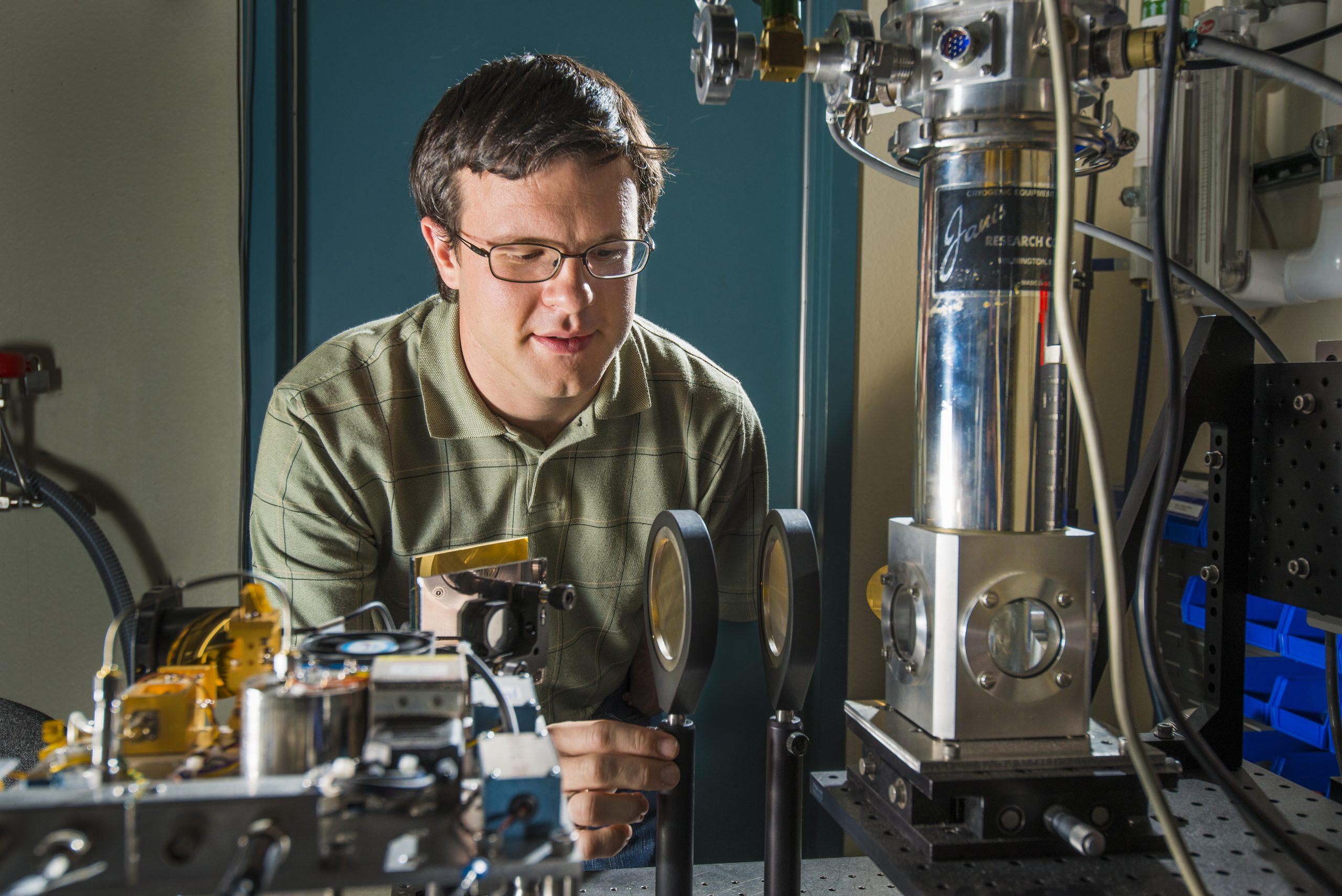
“Our experiment is more than a curiosity precisely because our plasma resonances are widely tunable,” says Sandia researcher Greg Dyer, co-primary investigator of a recently published online paper in Nature Photonics, expected to appear in print in that journal in November. “Usually, electromagnetically induced transparencies in more widely known systems like atomic gases, photonic crystals and metamaterials require tuning a laser’s frequencies to match a physical system. Here, we tune our system to match the radiation source. It’s inverting the problem, in a sense.”
The plasmonic crystal method could be used to shrink the size of photonic crystals, which are artificially built to allow transmission of specific wavelengths, and to develop tunable metamaterials, which require micron- or nano-sized bumps to tailor interactions between manmade structures and light. The plasmonic crystal, with its ability to direct light like a photonic crystal, along with its sub-wavelength, metamaterial-like size, in effect hybridizes the two concepts.
The crystal’s electron plasma forms naturally at the interface of semiconductors with different band gaps. It sloshes between their atomically smooth boundaries that, when properly aligned, form a crystal. Patterned metal electrodes allow its properties to be reconfigured, altering its light transmission range. In addition, defects intentionally mixed into the electron fluid allow light to be transmitted where the crystal is normally opaque.
However, this crystal won’t be coveted for the beauty of its light. The crystal transmits in the terahertz spectrum, a frequency range invisible to the human eye. Scientists also must adjust the crystal’s two-dimensional electron gas to electronically vary its output frequencies, something casual crystal buyers probably won’t be able to do.
Following online release, the paper titled, “Induced transparency by coupling of Tamm and defect states in tunable terahertz plasmonic crystals,” is slated to appear in the November print edition of Nature Photonics.
In addition to Dyer, other authors are co-principal investigator Eric Shaner, with Albert D. Grine, Don Bethke and John L. Reno, all from Sandia; Gregory R. Aizin of The City University of New York; and S. James Allen of the Institute for Terahertz Science and Technology at the University of California, Santa Barbara.
The work was supported by the Department of Energy’s Office of Basic Energy Sciences (BES) and performed in part at the Center for Integrated Nanotechnologies (CINT), a Sandia/Los Alamos national laboratories user facility that is one of the five DOE BES Nanoscale Science Research Centers that are premier national user facilities for interdisciplinary research at the nanoscale. Together the NSRCs comprise a suite of complementary facilities that provide researchers with state-of-the-art capabilities to fabricate, process, characterize and model nanoscale materials, and constitute the largest infrastructure investment of the National Nanotechnology Initiative. The NSRCs are located at DOE’s Argonne, Brookhaven, Lawrence Berkeley, Oak Ridge, Sandia and Los Alamos National Laboratories. For more information about the DOE NSRCs, click here.
