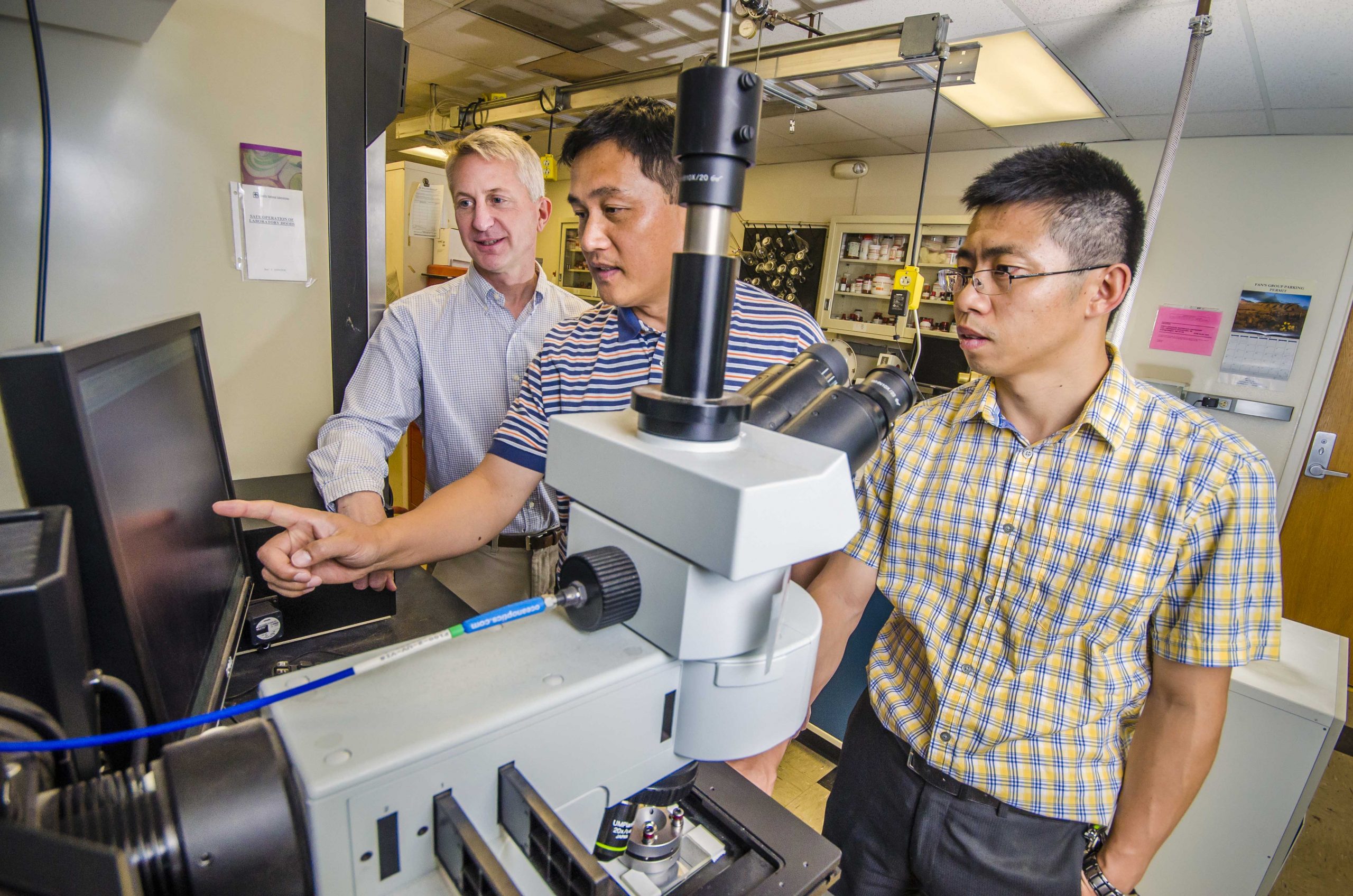
ALBUQUERQUE, N.M. — You wouldn’t think that mechanical force — the simple kind used to eject unruly patrons from bars, shoe a horse or emboss the raised numerals on credit cards — could process nanoparticles more subtly than the most advanced chemistry.

Yet, in a recent paper in Nature Communications, Sandia National Laboratories researcher Hongyou Fan and colleagues appear to have achieved a start toward that end.
Their newly patented and original method uses simple pressure — a kind of high-tech embossing — to produce finer and cleaner results in forming silver nanostructures than do chemical methods, which are not only inflexible in their results but leave harmful byproducts to dispose of.
Fan calls his approach “a simple stress-based fabrication method” that, when applied to nanoparticle arrays, forms new nanostructures with tunable properties.
“There is a great potential market for this technology,” he said. “It can be readily and directly integrated into current industrial manufacturing lines without creating new expensive and specialized equipment.”
Said Sandia co-author Paul Clem, “This is a foundational method that should enable a variety of devices, including flexible electronics such as antennas, chemical sensors and strain detectors.” It also would produce transparent electrodes for solar cells and organic light-emitting diodes, Clem said.
The method was inspired by industrial embossing processes in which a patterned mask is applied with high external pressure to create patterns in the substrate, Fan said. “In our technology, two diamond anvils were used to sandwich nanoparticulate thin films. This external stress manually induced transitions in the film that synthesized new materials,” he said.
The pressure, delivered by two diamond plates tightened by four screws to any controlled setting, shepherds silver nanospheres into any desired volume. Propinquity creates conditions that produce nanorods, nanowires and nanosheets at chosen thicknesses and lengths rather than the one-size-fits-all output of a chemical process, with no environmentally harmful residues.
While experiments reported in the paper were performed with silver — the most desirable metal because it is the most conductive, stable and optically interesting and becomes transparent at certain pressures — the method also has been shown to work with gold, platinum and other metallic nanoparticles
Clem said the researchers are now starting to work with semiconductors.
Bill Hammetter, manager of Sandia’s Advanced Materials Laboratory, said, “Hongyou has discovered a way to build one structure into another structure — a capability we don’t have now at the nanolevel. Eight or nine gigapascal —the amount of pressure at which phase change and new materials occur — are not difficult to reach. Any industry that has embossing equipment could lay a film of silver on a piece of paper, build a conductive pattern, then remove the extraneous material and be left with the pattern. A coating of nanoparticles that can build into another structure has a certain functionality we don’t have right now. It’s a discovery that hasn’t been commercialized, but could be done today with the same equipment used by anyone who makes credit cards.”
The method can be used to configure new types of materials. For example, under pressure, the dimensions of ordered three-dimensional nanoparticle arrays shrink. By fabricating a structure in which the sandwiching walls permanently provide that pressure, the nanoparticle array will remain at a constant state, able to transmit light and electricity with specific characteristics. This pressure-regulated fine-tuning of particle separation enables controlled investigation of distance-dependent optical and electrical phenomena.
At even higher pressures, nanoparticles are forced to sinter, or bond, forming new classes of chemically and mechanically stable nanostructures that no longer need restraining surfaces. These cannot be manufactured using current chemical methods.
Depending on the size, composition and phase orientation of the initial nanoparticle arrays, a variety of nanostructures or nanocomposites and 3-D interconnected networks are achievable.
The stress-induced synthesis processes are simple and clean. No thermal processing or further purification is needed to remove reaction byproducts.
This work was funded by the Department of Energy’s Office of Science. Other authors of the paper are from Cornell University and Los Alamos National Laboratory.
